Preliminary W91030B
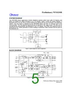
FUNCTIONAL DESCRIPTION
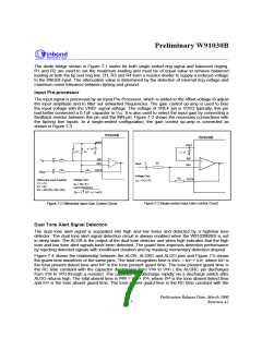
Figure 6 is shown functional blocks of W91030B. The device must operate with a 3.579545 MHz
system clock and consists four major functions and decribed as follows:
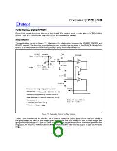
Ring Detector
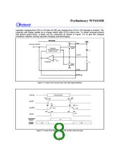
The application circuit in Figure 7-1 illustrates the relationship between the RNGDI, RNGRC and
RNGON signals. The three pin combination is used to detect an increase of the RNGDI voltage from
T+
ground to a level above the Schmitt trigger high going threshold voltage V
.
V
C1 = 0.1uF
DD
R1 = 470K
W91030B
Tip/A
R3 = 200 K
RNGDI
C1 = 0.1 uF
R4 = 300 K
Ring/B
R2 = 470 K
V
DD
R5 = 150 K
RNGRC
RNGON
C3 = 0.22 uF
Allowance minimal ring voltage (peak to peak) is:
Vpp
(max ring)
= 2 (V
T+(max) (R1 + R3 + R4) / R4 + 0.7)
Tolerance to noise between Tip and Ring and Vss is:
Vpeak (max noise)
Time constant is:
T+(min)
= V
(R1 + R3 + R4) / R4 + 0.7
R5 from 10K ohm to 500K ohm.
C3 from 47 nF to 0.68 uF.
DD
- V
DD
T+
T+
)]
T = R5 C3 ln [V
V
/ (V
T+(min)
<= V
<= V T+(max)
Figure 7-1. Application Circuit of the Ring Detecter
The RC time constant of the RNGRC pin is used to delay the output pulse of the RNGON pin for a
T+
low going edge on RNGDI. This edge goes from above the V voltage to the Schmitt trigger low
T-
going threshold voltage V . The RC time constant must be greater than the maximum period of the
ring signal, to ensure a minimum RNGON low interval and to filter the ring signal to get an envelope
output.
- 6 -

 WINBOND [ WINBOND ]