W90N745CD/W90N745CDG
Continued.
REGISTER
OFFSET R/W
DESCRIPTION
RESET VALUE
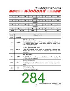
HSUART_IIR
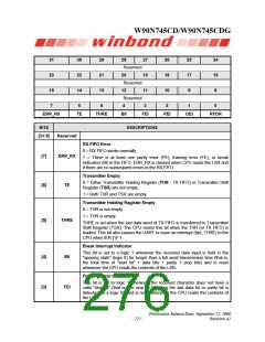
0x08
0x08
0x0C
0x10
0x14
0x18
0x1C
R
Interrupt Identification Register
0x8181_8181
HSUART_FCR
HSUART_LCR
HSUART_MCR
HSUART_LSR
HSUART_MSR
HSUART_TOR
W
FIFO Control Register
Undefined
R/W Line Control Register
0x0000_0000
0x0000_0000
0x6060_6060
0x0000_0000
0x0000_0000
R/W Modem Control Register (Optional)
R
R
Line Status Register
MODEM Status Register (Optional)
R/W Time Out Register
Note: Real register address = 0xFFF8_0000+ (UART number – 1) * (0x0100) + offset
NOTE: All of these registers are implemented 8-bit in UART design and it will be repeated 4 times
before send to APB bus. For example, when ARM CPU read register UART1_BRR, ARM CPU will get
UART1_RBR = {RBR[7:0], _RBR[7:0], RBR[7:0], RBR[7:0]}.
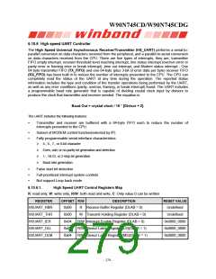
HSUART Receive Buffer Register (HSUART_RBR)
REGISTER
OFFSET R/W
DESCRIPTION
RESET VALUE
0x00
R
Receive Buffer Register (DLAB = 0)
Undefined
HSUART_RBR
31
23
15
7
30
22
14
6
29
21
13
5
28
Reserved
20
Reserved
12
Reserved
27
19
11
3
26
18
10
2
25
17
9
24
16
8
4
1
0
8-bit Received Data
BITS
DESCRIPTIONS
By reading this register, the UART will return an 8-bit data
received from SIN pin (LSB first).
[7:0]
8-bit Received Data
Publication Release Date: September 22, 2006
- 275 -
Revision A2

 WINBOND [ WINBOND ]