W90N745CD/W90N745CDG
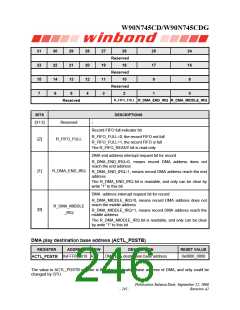
31
23
15
7
30
22
14
6
29
21
13
28
20
12
4
27
19
11
3
26
Reserved
18
25
17
9
24
16
8
Reserved
10
Reserved
2
5
1
0
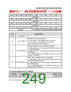
R_FIFO_FULL
R_DMA_END_IRQ R_DMA_MIDDLE_IRQ
Reserved
BITS
DESCRIPTIONS
[31:3]
Reserved
-
Record FIFO full indicator bit
R_FIFO_FULL=0, the record FIFO not full
R_FIFO_FULL=1, the record FIFO is full
The R_FIFO_READY bit is read only
[2]
[1]
R_FIFO_FULL
DMA end address interrupt request bit for record
R_DMA_END_IRQ=0, means record DMA address does not
reach the end address
R_DMA_END_IRQ
R_DMA_END_IRQ=1, means record DMA address reach the end
address
The R_DMA_END_IRQ bit is readable, and only can be clear by
write “1” to this bit
DMA address interrupt request bit for record
R_DMA_MIDDLE_IRQ=0, means record DMA address does not
reach the middle address
R_DMA_MIDDLE
_IRQ
[0]
R_DMA_MIDDLE_IRQ=1, means record DMA address reach the
middle address
The R_DMA_MIDDLE_IRQ bit is readable, and only can be clear
by write “1” to this bit
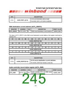
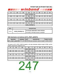
DMA play destination base address (ACTL_PDSTB)
REGISTER
ADDRESS
R/W
DESCRIPTION
RESET VALUE
0xFFF0_9018 R/W
DMA play destination base address
0x0000_0000
ACTL_PDSTB
The value in ACTL_PDSTB register is the play destination base address of DMA, and only could be
changed by CPU.
Publication Release Date: September 22, 2006
- 241 -
Revision A2

 WINBOND [ WINBOND ]