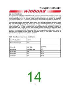
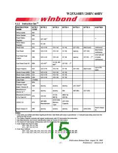
W25X10BV/20BV/40BV
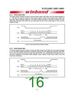
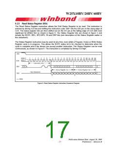
9.2.6 Write Status Register (01h)
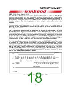
The Write Status Register instruction allows the Status Register to be written. A Write Enable
instruction must previously have been executed for the device to accept the Write Status Register
Instruction (Status Register bit WEL must equal 1). Once write enabled, the instruction is entered by
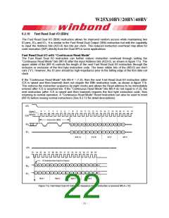
driving /CS low, sending the instruction code “01h”, and then writing the status register data byte as
illustrated in figure 7. The Status Register bits are shown in figure 3 and described earlier in this
datasheet.
Only non-volatile Status Register bits SRP, TB, BP2, BP1 and BP0 (bits 7, 5, 4, 3 and 2) can be
written to. All other Status Register bit locations are read-only and will not be affected by the Write
Status Register instruction.
The /CS pin must be driven high after the eighth bit of the last byte has been latched. If this is not
done the Write Status Register instruction will not be executed. After /CS is driven high, the self-timed
Write Status Register cycle will commence for a time duration of tW (See AC Characteristics). While
the Write Status Register cycle is in progress, the Read Status Register instruction may still accessed
to check the status of the BUSY bit. The BUSY bit is a 1 during the Write Status Register cycle and a
0 when the cycle is finished and ready to accept other instructions again. After the Write Register
cycle has finished the Write Enable Latch (WEL) bit in the Status Register will be cleared to 0.
The Write Status Register instruction allows the Block Protect bits (TB, BP2, BP1 and BP0) to be set
for protecting all, a portion, or none of the memory from erase and program instructions. Protected
areas become read-only (see Status Register Memory Protection table). The Write Status Register
instruction also allows the Status Register Protect bit (SRP) to be set. This bit is used in conjunction
with the Write Protect (/WP) pin to disable writes to the status register. When the SRP bit is set to a 0
state (factory default) the /WP pin has no control over the status register. When the SRP pin is set to a
1, the Write Status Register instruction is locked out while the /WP pin is low. When the /WP pin is
high the Write Status Register instruction is allowed.
Figure 7. Write Status Register Instruction Sequence Diagram
- 18 -

 WINBOND [ WINBOND ]