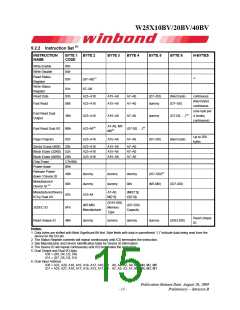
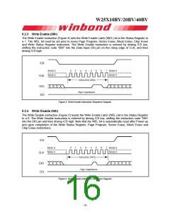
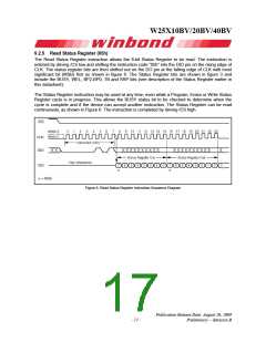
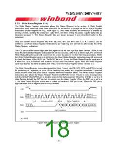
W25X10BV/20BV/40BV
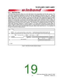
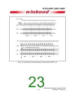
9.2.7 Read Data (03h)
The Read Data instruction allows one more data bytes to be sequentially read from the memory. The
instruction is initiated by driving the /CS pin low and then shifting the instruction code “03h” followed
by a 24-bit address (A23-A0) into the DIO pin. The code and address bits are latched on the rising
edge of the CLK pin. After the address is received, the data byte of the addressed memory location
will be shifted out on the DO pin at the falling edge of CLK with most significant bit (MSB) first. The
address is automatically incremented to the next higher address after each byte of data is shifted out
allowing for a continuous stream of data. This means that the entire memory can be accessed with a
single instruction as long as the clock continues. The instruction is completed by driving /CS high. The
Read Data instruction sequence is shown in figure 8. If a Read Data instruction is issued while an
Erase, Program or Write cycle is in process (BUSY=1) the instruction is ignored and will not have any
effects on the current cycle. The Read Data instruction allows clock rates from D.C. to a maximum of
fR (see AC Electrical Characteristics).
Figure 8. Read Data Instruction Sequence Diagram
Publication Release Date: August 20, 2009
- 19 -
Preliminary -- Revision B

 WINBOND [ WINBOND ]