W25X10BV/20BV/40BV
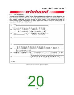
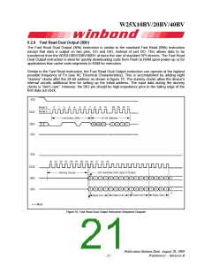
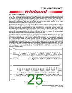
9.2.9 Fast Read Dual Output (3Bh)
The Fast Read Dual Output (3Bh) instruction is similar to the standard Fast Read (0Bh) instruction
except that data is output on two pins, DO and DIO, instead of just DO. This allows data to be
transferred from the W25X10BV/20BV/40BV at twice the rate of standard SPI devices. The Fast Read
Dual Output instruction is ideal for quickly downloading code from Flash to RAM upon power-up or for
applications that cache code-segments to RAM for execution.
Similar to the Fast Read instruction, the Fast Read Dual Output instruction can operate at the highest
possible frequency of FR (see AC Electrical Characteristics). This is accomplished by adding eight
“dummy” clocks after the 24-bit address as shown in figure 10. The dummy clocks allow the device's
internal circuits additional time for setting up the initial address. The input data during the dummy
clocks is “don’t care”. However, the DIO pin should be high-impedance prior to the falling edge of the
first data out clock.
Figure 10. Fast Read Dual Output Instruction Sequence Diagram
Publication Release Date: August 20, 2009
- 21 -
Preliminary -- Revision B

 WINBOND [ WINBOND ]