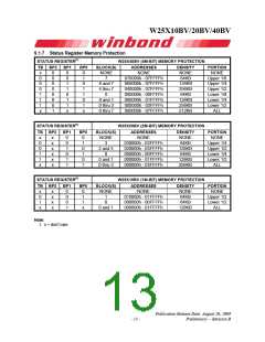
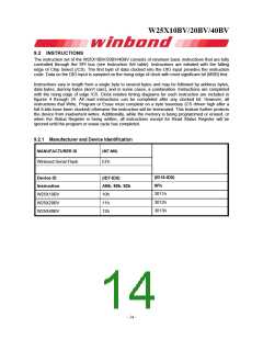
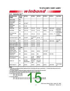
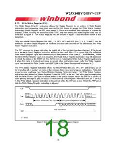
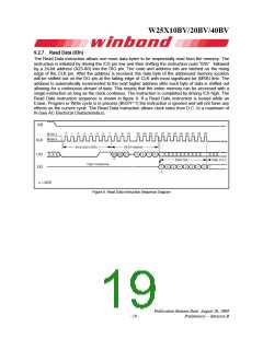
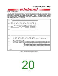
W25X10BV/20BV/40BV
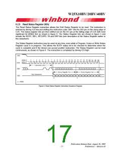
9.2.5 Read Status Register (05h)
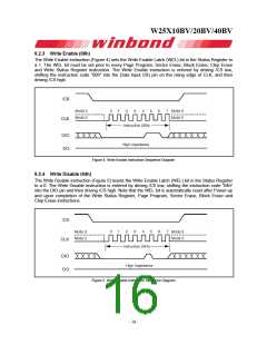
The Read Status Register instruction allows the 8-bit Status Register to be read. The instruction is
entered by driving /CS low and shifting the instruction code “05h” into the DIO pin on the rising edge of
CLK. The status register bits are then shifted out on the DO pin at the falling edge of CLK with most
significant bit (MSB) first as shown in figure 6. The Status Register bits are shown in figure 3 and
include the BUSY, WEL, BP2-BP0, TB and SRP bits (see description of the Status Register earlier in
this datasheet).
The Status Register instruction may be used at any time, even while a Program, Erase or Write Status
Register cycle is in progress. This allows the BUSY status bit to be checked to determine when the
cycle is complete and if the device can accept another instruction. The Status Register can be read
continuously, as shown in Figure 6. The instruction is completed by driving /CS high.
Figure 6. Read Status Register Instruction Sequence Diagram
Publication Release Date: August 20, 2009
- 17 -
Preliminary -- Revision B

 WINBOND [ WINBOND ]