W25X10BV/20BV/40BV
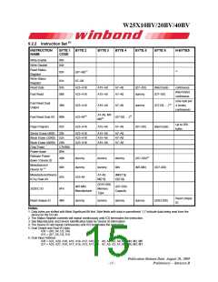
9.2.2 Instruction Set (1)
INSTRUCTION
NAME
BYTE 1 BYTE 2
CODE
BYTE 3
BYTE 4
BYTE 5
BYTE 6
N-BYTES
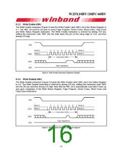
Write Enable
06h
04h
Write Disable
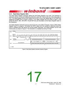
Read Status
Register
(2)
05h
(S7–S0)(1)
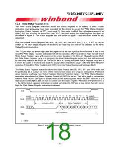
Write Status
Register
01h
03h
0Bh
S7–S0
Read Data
A23–A16
A23–A16
A15–A8
A15–A8
A7–A0
A7–A0
(D7–D0)
dummy
(Next byte)
(D7–D0)
continuous
(Next Byte)
continuous
(one byte per
Fast Read
Fast Read Dual
Output
3Bh
BBh
A23–A16
A15–A8
A7–A0
dummy
(D7-D0, …)(5) 4 clocks,
continuous)
A7-A0, M7-
M0(6)
Fast Read Dual I/O
A23-A8(6)
A23–A16
(D7-D0, …)(5)
A7–A0
Up to 256
(Next byte)
Page Program
02h
20h
A15–A8
(D7–D0)
bytes
Sector Erase (4KB)
A23–A16
A23–A16
A23–A16
A15–A8
A15–A8
A15–A8
A7–A0
A7–A0
A7–A0
Block Erase (32KB) 52h
Block Erase (64KB) D8h
Chip Erase
C7h/60h
Power-down
B9h
Release Power-
down / Device ID
Manufacturer/
Device ID (3)
ABh
dummy
dummy
dummy
dummy
dummy
00h
(ID7-ID0)(4)
(M7-M0)
90h
92h
(ID7-ID0)
Manufacturer/Device
ID by Dual I/O
A7-A0,
M[7:0]
(MF[7:0],
ID[7:0])
A23-A8
(ID15-ID8)
Memory
Type
(M7-M0)
(ID7-ID0)
Capacity
JEDEC ID
9Fh
4Bh
Manufacturer
Read Unique
Read Unique ID
dummy
dummy
dummy
dummy
(ID63-ID0)
ID
Notes:
1. Data bytes are shifted with Most Significant Bit first. Byte fields with data in parenthesis “( )” indicate data being read from the
device on the DO pin.
2. The Status Register contents will repeat continuously until /CS terminates the instruction.
3. See Manufacturer and Device Identification table for Device ID information.
4. The Device ID will repeat continuously until /CS terminates the instruction.
5. Dual Output and Dual I/O data
IO0 = (D6, D4, D2, D0)
IO1 = (D7, D5, D3, D1)
6. Dual Input Address
IO0 = A22, A20, A18, A16, A14, A12, A10, A8 A6, A4, A2, A0, M6, M4, M2, M0
IO1 = A23, A21, A19, A17, A15, A13, A11, A9 A7, A5, A3, A1, M7, M5, M3, M1
Publication Release Date: August 20, 2009
- 15 -
Preliminary -- Revision B

 WINBOND [ WINBOND ]