W25X10BV/20BV/40BV
9.
CONTROL AND STATUS REGISTERS
The Read Status Register instruction can be used to provide status on the availability of the Flash
memory array, if the device is write enabled or disabled, and the state of write protection. The Write
Status Register instruction can be used to configure the device write protection features. See Figure 3.
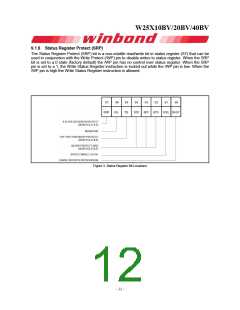
9.1 STATUS REGISTER
9.1.1 BUSY
BUSY is a read only bit in the status register (S0) that is set to a 1 state when the device is executing
a Page Program, Sector Erase, Block Erase, Chip Erase or Write Status Register instruction. During
this time the device will ignore further instructions except for the Read Status Register instruction (see
tW, tPP, tSE, tBE, and tCE in AC Characteristics). When the program, erase or write status register
instruction has completed, the BUSY bit will be cleared to a 0 state indicating the device is ready for
further instructions.
9.1.2 Write Enable Latch (WEL)
Write Enable Latch (WEL) is a read only bit in the status register (S1) that is set to a 1 after executing
a Write Enable Instruction. The WEL status bit is cleared to a 0 when the device is write disabled. A
write disable state occurs upon power-up or after any of the following instructions: Write Disable, Page
Program, Sector Erase, Block Erase, Chip Erase and Write Status Register.
9.1.3 Block Protect Bits (BP2, BP1, BP0)
The Block Protect Bits (BP2, BP1, and BP0) are non-volatile read/write bits in the status register (S4,
S3, and S2) that provide Write Protection control and status. Block Protect bits can be set using the
Write Status Register Instruction (see tW in AC characteristics). All, none or a portion of the memory
array can be protected from Program and Erase instructions (see Status Register Memory Protection
table). The factory default setting for the Block Protection Bits is 0, none of the array protected. The
Block Protect bits can not be written to if the Status Register Protect (SRP) bit is set to 1 and the Write
Protect (/WP) pin is low.
9.1.4 Top/Bottom Block Protect (TB)
The Top/Bottom bit (TB) controls if the Block Protect Bits (BP2, BP1, BP0) protect from the Top
(TB=0) or the Bottom (TB=1) of the array as shown in the Status Register Memory Protection table.
The TB bit is non-volatile and the factory default setting is TB=0. The TB bit can be set with the Write
Status Register Instruction provided that the Write Enable instruction has been issued. The TB bit can
not be written to if the Status Register Protect (SRP) bit is set to 1 and the Write Protect (/WP) pin is
low.
9.1.5 Reserved Bits
Status register bit location S6 is reserved for future use. Current devices will read 0 for this bit
location. It is recommended to mask out the reserved bit when testing the Status Register. Doing this
will ensure compatibility with future devices.
Publication Release Date: August 20, 2009
- 11 -
Preliminary -- Revision B

 WINBOND [ WINBOND ]