WED3DL644V
White Electronic Designs
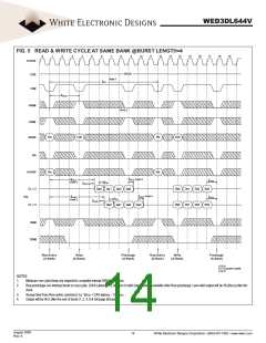
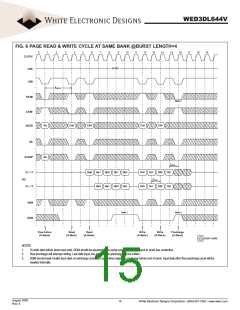
FIG. 6 PAGE READ & WRITE CYCLE AT SAME BANK @BURST LENGTH=4
0
1
2
3
4
5
6
7
8
9
10
11
12
13
14
15
16
17
18
19
CLOCK
HIGH
CKE
CE#
tRCD
RAS#
Note 2
CAS#
ADDR
Ra
Ca0
Cb0
Cc0
Cd0
BA
A10/AP
CL = 2
Ra
tRDL
Qa0
Qa1
Qb0
Qa1
Qb1
Qb0
Qb2
Dc0
Dc0
Dc1
Dd0
Dd0
Dd1
DQ
tCDL
CL = 3
Qa0
Qb1
Dc1
Dd1
WE#
DQM
Note 1
Note 3
Row Active
(A-Bank)
Read
(A-Bank)
Read
(A-Bank)
Write
(A-Bank)
Write
(A-Bank)
Precharge
(A-Bank)
DON'T CARE
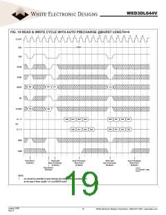
NOTES:
1.
2.
3.
To write data before burst read ends, DQM should be asserted three cycles prior to write command to avoid bus contention.
Row precharge will interrupt writing. Last data input, tRDL before Row precharge, will be written.
DQM should mask invalid input data on precharge command cycle when asserting precharge before end of burst. Input data after Row precharge cycle will be
masked internally.
August 2005
Rev. 6
15
White Electronic Designs Corporation • (602) 437-1520 • www.wedc.com

 WEDC [ WHITE ELECTRONIC DESIGNS CORPORATION ]