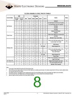
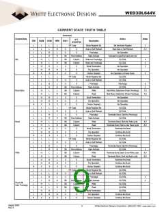
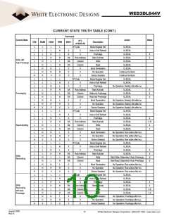
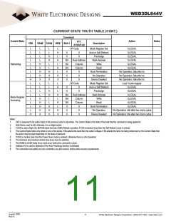
WED3DL644V
White Electronic Designs
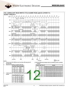
FIG. 3 SINGLE BIT READ-WRITE CYCLE (SAME PAGE) @CAS LATENCY=3,
BURST LENGTH=1
0
1
2
3
4
5
6
7
8
9
10
11
12
13
14
15
16
17
18
19
CLOCK
tCH
tCL
tCC
HIGH
CKE
tRCD
tRAS
CE#
tSS
tSH
tRCD
tRP
tSS
tSH
RAS#
tCCD
tSS
tSH
CAS#
ADDR
tSS
tSH
tSS
tSH
Ra
Ca
Cb
Cc
Rb
Note 2
BS
Note 2, 3
BS
Note 2, 3
BS
Note 2, 3 Note 4
BS
Note 2
BS
BA
A10/AP
DQ
BS
Ra
Note 3
Note 3
Db
Note 3 Note 4
Rb
tRAC
tSS
tSS
tSS
tSH
tSH
tSH
tSAC
Qa
Qc
tSLZ
tOH
WE#
DQM
Row Active
Read
Write
Read
Row Active
DON'T CARE
Precharge
NOTES:
1.
All input except CKE & DQM can be don't care when CE# is high at the CK
high going edge.
Bank active & read/write are controlled by BA0~BA1.
3. Enable and disable auto precharge function are controlled by A10/AP in read/write
command.
2.
A10/AP BA0
BA1
0
Operation
BA0 BA1 Active & Read/Write
0
Distribute auto precharge, leave bank A active at end of burst.
Disable auto precharge, leave bank B active at end of burst.
Disable auto precharge, leave bank C active at end of burst.
Disable auto precharge, leave bank D active at end of burst.
Enable auto precharge, precharge bank A at end of burst.
Enable auto precharge, precharge bank B at end of burst.
Enable auto precharge, precharge bank C at end of burst.
Enable auto precharge, precharge bank D at end of burst.
0
0
1
1
0
1
0
1
Bank A
Bank B
Bank C
Bank D
0
1
0
1
0
1
0
1
0
4.
A10/AP and BA0~BA1 control bank precharge when precharge command is
asserted.
0
1
1
1
0
A10/AP BA0 BA1 Precharge
1
1
0
0
0
0
1
0
0
1
1
x
0
1
0
1
x
Bank A
Bank B
Bank C
Bank D
All Banks
August 2005
Rev. 6
12
White Electronic Designs Corporation • (602) 437-1520 • www.wedc.com

 WEDC [ WHITE ELECTRONIC DESIGNS CORPORATION ]