Preliminary
VG37648041AT
256M:x4, x8, x16
VIS
CMOS Synchronous Dynamic RAM
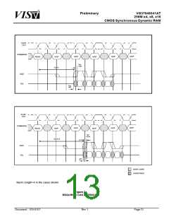
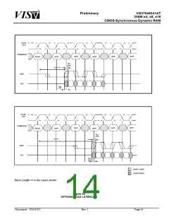
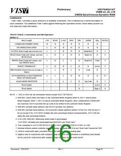
Accesses within a given burst may be programmed to be either sequential or interleaved; this is referred
to as the burst type and is selected via bit M3.
The ordering of accesses within a burst is determined by the burst length, the burst type and the starting
column address, as shown in Table 1.
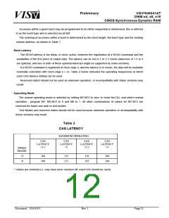
Read Latency
The READ latency is the delay, in clock cycles, between the registration of a READ command and the
availability of the first piece of output data. The latency can be set to 2 or 2.5 clocks (latencies of 1.5 or 3
are optional, and one or both of these optional latencies might be supported by some vendors).
If a READ command is registered at clock edge n, and the latency is m clocks, the data will be available
nominally coincident with clock edge n + m. Table 2 below indicated the operating frequencies at which
each CAS latency setting can be used.
Reserved stated should not be used as unknown operation, or incompatibility with future versions may
result.
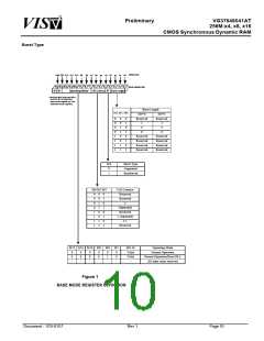
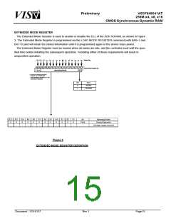
Operating Mode
The normal operating mode is selected by setting M7-M12 to zero; to reset the DLL and select normal
operation , program M7, M9-M12 to 0 and M8 to 1. All other combinations of values for M7-M12 are
reserved for future use and/ or test modes.
Test Modes and reserved states should not be used because unknown operation or incompatibility with
future versions may result.
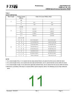
Table 2
CAS LATENCY
MAXIMUM OPERATING
CAS
LATENCY
=1.5
CAS
LATENCY
=2
CAS
LATENCY
=2.5
CAS
LATENCY
=3
SPEED
GRADE
-75
-8
100
100
133
125
150
143
200
166
* Values are nominal (i.e. may have been rounded off; exact tCK should be used)
Document : 1G5-0157
Rev.1
Page12

 VML [ VANGUARD INTERNATIONAL SEMICONDUCTOR ]