Preliminary
VG37648041AT
256M:x4, x8, x16
VIS
CMOS Synchronous Dynamic RAM
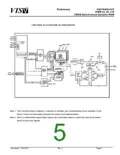
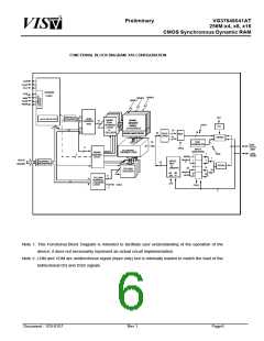
Note: The functionality described in, and the timing specifications included in this data
sheet are for the DLL Enabled mode of operation. This is the only normal operating
mode for these DDR devices.
Features
• Double-data-rate architecture: two data transfers per clock cycle
• Bidirectional, intermittent data strobe (DQS) is transmitted/received with data, to be used in
capturing data at the receiver
• DQS is edge-aligned with data for READs: center-aligned with data for WRITEs
• Differential clock inputs (CLK and CLK#)
• DLL aligns DQ and DQS transitions with CLK transitions
• Commands entered on each positive CLK edge; data referenced to both edges of DQS
• Four internal banks for concurrent operation
• Data mask (DM) for write data
• Burst lengths:2,4, or 8
• CAS Latency: 2 or 2.5
• AUTO PRECHARGE option for each burst access
• Auto Refresh and Self Refresh Modes
• 7.81us Auto Refresh Interval
• 2.5V (SSTL_2 compatible) I/O
• VDDQ=+2.5V ±0.2V
• VDD=+3.3V ±0.3V
Document : 1G5-0157
Rev.1
Page2

 VML [ VANGUARD INTERNATIONAL SEMICONDUCTOR ]