VSC8601 Datasheet
Configuration
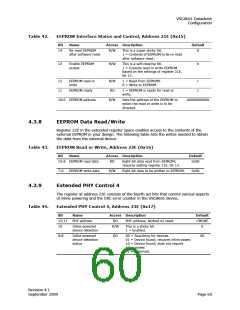
4.3.14
Ethernet Packet Generator Control 2
The register at address 30E consists of the second of bits that provide access to and
control over various aspects of the EPG testing feature. For information about the first
set of EPG control bits, see Table 47, page 63. The following table lists the settings
available.
Table 48.
EPG Control Register 2, Address 30E (0x1E)
Bit
Name
Access Description
R/W Data pattern repeated in the payload of
packets generated by the EPG
Default
15:0 EPG packet payload
0x00
Note If any of bits 15:0 in this register are changed while the EPG is running (bit 14
of register 29E is set to 1), that bit (29E.14) must first be cleared and then set back to
1 for the change to take effect and to restart the EPG.
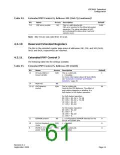
4.4
CMODE
The information in this section consists of a detailed description of the methods to
configure the VSC8601 device using its CMODE pins. It includes descriptions of the
registers that work together with the CMODE pins to control the device function.
There are four configuration mode (CMODE) pins on the VSC8601 device. For more
information about the physical location of the CMODE pins, see “Pin Descriptions,”
page 84. Each CMODE pin maps to a configuration bit, which means there are 16
possible settings for the device.
4.4.1
CMODE Pins and Related Functions
The following table lists the pin numbers and device functionality that is controlled by
each configuration bit.
Table 49.
CMODE Configuration Pins and Device Functions
CMODE Pin Bit 3 (MSB) Control Bit 2 Controls
Bit 1 Controls
Bit 0 (LSB) Controls
3
PHY address [3]
PHY address [4]
MAC calibration
setting[1]
MAC calibration
setting[0]
2
1
PHY address [2]
PHY address [1]
ActiPHY
RGMII clock skew[1]
RGMII clock skew[0]
Link speed downshift
Speed/Duplex Modes
[1]
Speed/Duplex modes [0]
0
PHY address [0]
CLKOUT enable
Advertise asymmetric
pause
Advertise symmetric
pause
Revision 4.1
September 2009
Page 64

 VITESSE [ VITESSE SEMICONDUCTOR CORPORATION ]