VSC8601 Datasheet
Configuration
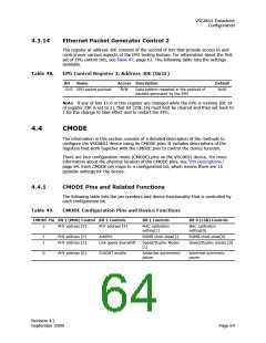
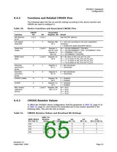
4.4.2
Functions and Related CMODE Pins
The following table lists the pin and bit settings according to the device function and
CMODE pin used to configure it.
Table 50.
Device Functions and Associated CMODE Pins
CMODE
Pin
Associated
Register, Bit Result
Function
Bit
PHY Address
[4:0]
3 to 0
3 and 2
Sets the PHY address.
Link speed
downshift
1
2
Register 20E, 0 = Link only according to the auto-negotiation
bit 4
resolution.
1 = Enable link speed downshift feature.
Speed and
duplex
1
2
1 and 0
Register 4,
bits 8:5 and
Register 9,
bits 9:8
00 = 10/100/1000BASE-T FDX/HDX.
01 = 10/100/1000BASE-T FDX; 10/100BASE-T HDX.
10 = 1000BASE-T FDX only.
11 = 10/100BASE-T FDX/HDX.
RGMII clock
skew
1 and 0
Register 23,
bit 8
00 = No skew on RX_CLK and TX_CLK.
01 = 1.4 ns skew on RX_CLK and TX_CLK.
10 = 1.7 ns skew on RX_CLK and TX_CLK.
11 = 2.0 ns skew on RX_CLK and TX_CLK.
Advertise
asymmetric
pause
0
0
1
0
Register 4,
bit 11
0 = Not advertised.
1 = Advertised.
Advertise
symmetric
pause
Register 4,
bit 10
0 = Not advertised.
1 = Advertised.
CLKOUT enable
0
2
3
2
2
Register 18,
bit 0
0 = Disabled.
1 = Enabled.
ActiPHY
Register 23,
bit 5
0 = Disabled.
1 = Enabled.
MAC resistor
calibration
setting
1 and 0
Register 19E, 00 = 50 Ω.
bits 15:14
01 = 60 Ω.
10 = 30 Ω.
11 = 45 Ω.
4.4.3
CMODE Resistor Values
To affect the VSC8601 device configuration, find the parameter in Table 49, page 64 or
in Table 50, page 65, and connect the associated pin to the resistor specified in the
following table. This sets the bits as shown.
Table 51.
CMODE Resistor Values and Resultant Bit Settings
With 1%
With CMODE
Pin Tied To
Resistor
Value
Set
Set
Bit 2 to:
Set
Bit 1 to:
Set
Bit 3 (MSB) to:
Bit 0 (LSB) to:
VSS
VSS
VSS
VSS
0
0
0
0
0
0
0
0
0
0
0
1
1
0
1
0
1
2.26 kΩ
4.02 kΩ
5.90 kΩ
Revision 4.1
September 2009
Page 65

 VITESSE [ VITESSE SEMICONDUCTOR CORPORATION ]