VSC8601 Datasheet
Configuration
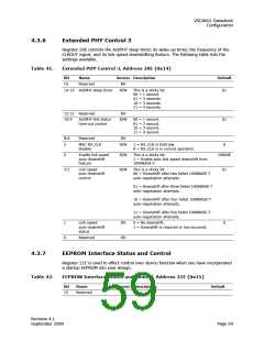
Table 42.
EEPROM Interface Status and Control, Address 21E (0x15)
Bit
Name
Access Description
Default
14
Re-read EEPROM
after software reset
R/W
R/W
This is a super-sticky bit.
1 = Contents of EEPROM to be re-read
after software reset.
0
13
Enable EEPROM
access
This is a self-clearing bit.
1 = Execute read or write EEPROM
based on the settings of register 21E,
bit 12.
0
12
11
EEPROM read or
write
R/W
RO
1 = Read from EEPROM.
0 = Write to EEPROM.
1
EEPROM ready
1 = EEPROM is ready for read or
write.
1
10:0 EEPROM address
R/W
Sets the address of the EEPROM to
which the read or write is to be
directed.
00000000000
4.3.8
EEPROM Data Read/Write
Register 22E in the extended register space enables access to the contents of the
external EEPROM in your design. The following table lists the writes needed to obtain
the data from the external device.
Table 43.
EEPROM Read or Write, Address 22E (0x16)
Bit
Name
Access Description
Default
15:8 EEPROM read data
RO
Eight-bit data read from EEPROM;
0x00
requires setting register 21E, bit 13.
7:0
EEPROM write data
R/W
Eight-bit data to be written to EEPROM.
0x00
4.3.9
Extended PHY Control 4
The register at address 23E consists of the fourth set bits that control various aspects
of inline powering and the CRC error counter in the VSC8601 device.
Table 44.
Extended PHY Control 4, Address 23E (0x17)
Bit
Name
Access Description
Default
CMODE
0
15:11
10
PHY address
RO
PHY address; latched on reset.
Inline powered
device detection
R/W
This is a sticky bit.
1 = Enabled.
9:8
Inline powered
device detection
status
RO
00 = Searching for devices.
01 = Device found; requires inline power.
10 = Device found; does not require
inline power.
00
11 = Reserved.
Revision 4.1
September 2009
Page 60

 VITESSE [ VITESSE SEMICONDUCTOR CORPORATION ]