VSC8601 Datasheet
Configuration
required to be able to write to the EEPROM, refer to the EEPROM’s specific datasheet to
ensure that write protection on the EEPROM is not set.
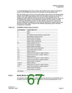
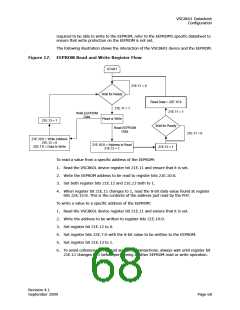
The following illustration shows the interaction of the VSC8601 device and the EEPROM.
Figure 17.
EEPROM Read and Write Register Flow
START
21E.11 = 0
Wait for Ready
Read Data = 22E.15:8
21E.11 = 1
21E.11 = 1
Write EEPROM
Data
Read or Write
21E.13 = 1
Wait for Ready
Read EEPROM
Data
21E.11 = 0
21E.10:0 = Write Address
21E.12 = 0
22E.7:0 = Data to Write
21E.10:0 = Address to Read
21E.12 = 1
21E.13 = 1
To read a value from a specific address of the EEPROM:
1. Read the VSC8601 device register bit 21E.11 and ensure that it is set.
2. Write the EEPROM address to be read to register bits 21E.10:0.
3. Set both register bits 21E.12 and 21E.13 both to 1.
4. When register bit 21E.11 changes to 1, read the 8-bit data value found at register
bits 22E.15:8. This is the contents of the address just read by the PHY.
To write a value to a specific address of the EEPROM:
1. Read the VSC8601 device register bit 21E.11 and ensure that it is set.
2. Write the address to be written to register bits 21E.10:0.
3. Set register bit 21E.12 to 0.
4. Set register bits 22E.7:0 with the 8-bit value to be written to the EEPROM.
5. Set register bit 21E.13 to 1.
6. To avoid collisions during read and write transactions, always wait until register bit
21E.11 changes to 1 before performing another EEPROM read or write operation.
Revision 4.1
September 2009
Page 68

 VITESSE [ VITESSE SEMICONDUCTOR CORPORATION ]