VSC8601 Datasheet
Configuration
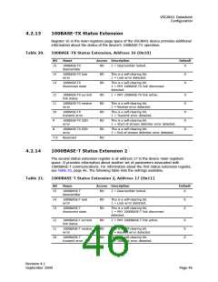
Table 21.
1000BASE-T Status Extension 2, Address 17 (0x11) (continued)
Bit
Name
Access Description
Default
9
1000BASE-T SSD
error
RO
RO
RO
RO
This is a self-clearing bit.
1 = Start-of-stream delimiter error detected.
0
8
7
6
1000BASE-T ESD
error
This is a self-clearing bit.
1 = End-of-stream delimiter error detected.
0
0
0
0
1000BASE-T carrier
extension error
This is a self-clearing bit.
1 = Carrier extension error detected.
Non-compliant
BCM5400 detected
1 = Non-compliant BCM5400 detected.
1 = MDI crossover error detected.
5
MDI crossover error
Reserved
RO
RO
4:0
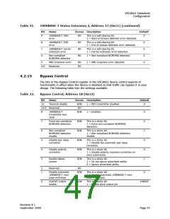
4.2.15
Bypass Control
The bits in the Bypass Control register in the VSC8601 device control aspects of
functionality in effect when the device is disabled so that traffic can bypass it in your
design. The following table lists the settings available.
Table 22.
Bypass Control, Address 18 (0x12)
Bit
Name
Access Description
Default
15
Transmit disable
R/W
RO
1 = PHY transmitter disabled.
0
14:9 Reserved
8
7
6
5
4
3
1000BASE-T
transmitter test
clock
R/W
1 = Enabled.
0
0
1
0
0
1
Force non-compliant
BCM5400 detection
R/W
R/W
R/W
R/W
R/W
This is a sticky bit.
1 = Force non-compliant BCM5400
detection.
Non-compliant
BCM5400 detection
disable
This is a sticky bit.
1 = Non-compliant BCM5400 detection
disable.
Disable pair swap
correction
This is a sticky bit.
1 = Disable the automatic pair swap
correction.
Disable polarity
correction
This is a sticky bit.
1 = Disable polarity inversion correction on
each subchannel.
Parallel detect
control
This is a sticky bit.
1 = Do not ignore advertised ability.
0 = Ignore advertised ability.
2
1
Reserved
RO
Disable automatic
1000BASE-T next
page exchange
R/W
This is a sticky bit.
1 = Disable automatic 1000BASE-T next
page exchanges.
0
0
CLKOUT output
enable
R/W
This is a sticky bit.
1 = Enable clock output pin.
CMODE
Revision 4.1
September 2009
Page 47

 VITESSE [ VITESSE SEMICONDUCTOR CORPORATION ]