TMC8462 Datasheet • Document Revision V1.4 • 2018-May -09
161 / 204
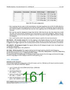
Clock polarity Clock phase SPI mode MOSI change
MISO sample
0
0
1
1
0
1
0
1
0
1
2
3
SCK falling edge SCK rising edge
SCK rising edge
SCK rising edge
SCK falling edge
SCK falling edge
SCK falling edge SCK rising edge
Table 198: SPI mode configuration
•
•
Bit 4 reverses the bit order in the transmission, the least significant bit of SPI_TX_DATA (Bit 0) is
transmitted first, the least significant bit of SPI_RX_DATA is the first received bit, the most significant
bit of SPI_TX_DATA is transmitted last and the most significant bit of SPI_RX_DATA is the last bit
received.
Bit 3 can be used for datagrams longer than 64 bit. With this bit set, the chip select line is held
low after the transmission, allowing more transmissions in the same datagram. Before the last
transmission, this bit must be set to 0 again so that the chip select line goes high afterwards, ending
the datagram.
• Bits 1 and 0 define which chip select line (which slave) is used for the next transmission.
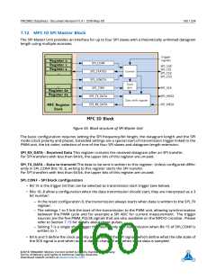
SPI_STATUS – SPI transfer status Bit 0 of this register is the Ready indicator for the SPI master unit.
When this bit is set, a new transfer can be started. When this bit is 0 and the start of a new transfer
is triggered, the trigger is ignored, the currently active transfer is finished but the new transfer is not started.
SPI_LENGTH – SPI datagram length This register defines the SPI datagram length in bits. Any length from
1 to 64 bits is possible.
SPI datagram length (bits) = SPI_LENGTH+1
SPI_TIME – SPI bit duration This register defines the bit length and thus the SPI clock frequency.
The duration of one SPI clock cycle can be calculated as tSCK = (4+(2*SPI_TIME))/25MHz = (4+(2*SPI_TIME))*40ns,
the SPI clock frequency is fSCK = 25MHz/(4+(2*SPI_TIME)).
The delay between the falling edge of CSN (becoming active) and the first SCK edge and the last SCK edge
and the rising edge of CSN is always a half SCK clock cycle (tSCK/2).
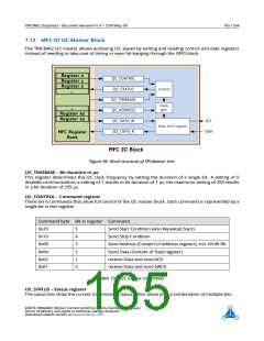
7.12.1 SPI Examples
TMC262 on SPI channel 0
This example shows the configuration of the SPI master unit for a TMC262 as SPI slave 0 and the transfer
of data to the TMC262’s DRVCONF register.
1. Use 3.125 MHz SPI clock (25MHz/(4+(2*2))) = (25MHz/8)
SPI_TIME <= 0x02
2. Use 20 bit datagrams
SPI_LENGTH <= 0x13
3. Start on TX write, SPI-Mode 3, MSB first, single datagrams, Slave 0)
SPI_CONF <= 0x0060
4. Wait until SPI-Master is ready
while (SPI_STATUS & 0x01 != 0x01)
©2018 TRINAMIC Motion Control GmbH & Co. KG, Hamburg, Germany
Terms of delivery and rights to technical change reserved.
Download newest version at www.trinamic.com

 TRINAMIC [ TRINAMIC MOTION CONTROL GMBH & CO. KG. ]