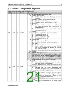
TMC6200 DATASHEET (Rev. 1.01 / 2018-NOV-15)
17
4 SPI Interface
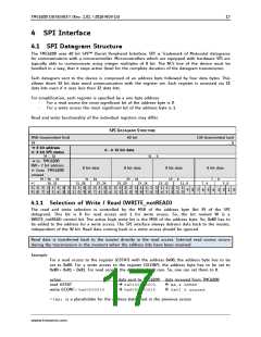
4.1 SPI Datagram Structure
The TMC6200 uses 40 bit SPI™ (Serial Peripheral Interface, SPI is Trademark of Motorola) datagrams
for communication with a microcontroller. Microcontrollers which are equipped with hardware SPI are
typically able to communicate using integer multiples of 8 bit. The NCS line of the device must be
handled in a way, that it stays active (low) for the complete duration of the datagram transmission.
Each datagram sent to the device is composed of an address byte followed by four data bytes. This
allows direct 32 bit data word communication with the register set. Each register is accessed via 32
data bits even if it uses less than 32 data bits.
For simplification, each register is specified by a one byte address:
-
-
For a read access the most significant bit of the address byte is 0.
For a write access the most significant bit of the address byte is 1.
Read and write functionality of the individual registers may differ.
SPI DATAGRAM STRUCTURE
MSB (transmitted first)
40 bit
LSB (transmitted last)
... 0
39 ...
→ 8 bit address
8 bit SPI status
39 ... 32
→ 32 bit data
31 ... 0
→ to TMC6200
RW + 7 bit address
from TMC6200
unused
8 bit data
31 ... 24
8 bit data
23 ... 16
8 bit data
15 ... 8
8 bit data
7 ... 0
39 / 38 ... 32
W
38...32
31...28
27...24
23...20
19...16
15...12
11...8
7...4
3...0
3 3 3 3 3 3 3 3 3 3 2 2 2 2 2 2 2 2 2 2 1 1 1 1 1 1 1 1 1 1
9 8 7 6 5 4 3 2 1 0 9 8 7 6 5 4 3 2 1 0 9 8 7 6 5 4 3 2 1 0
9 8 7 6 5 4 3 2 1 0
4.1.1 Selection of Write / Read (WRITE_notREAD)
The read and write selection is controlled by the MSB of the address byte (bit 39 of the SPI
datagram). This bit is 0 for read access and 1 for write access. So, the bit named W is a
WRITE_notREAD control bit. The active high write bit is the MSB of the address byte. So, 0x80 has to
be added to the address for a write access. The SPI interface always delivers data back to the master,
independent of the W bit. Read data coming back in a write access should be ignored.
Read data is transferred back to the master directly in the read access. Internal read access occurs
during the transmission in the moment when the address bits have been received.
Example:
For a read access to the register (GSTAT) with the address 0x00, the address byte has to be
set to 0x00. For a write access to the register (GCONF), the address byte has to be set to
0x80 + 0x01 = 0x81. For read access, the data bits don’t care. So, one can set them to 0.
action
read GSTAT
data sent to TMC6200 data received from TMC6200
→ 0x0100000000
AA & GSTAT
write GCONF:= 0x00000010
→ 0x8000000010
0x01 & unused
*)AA: is a placeholder for the address byte used in the previous access
www.trinamic.com

 TRINAMIC [ TRINAMIC MOTION CONTROL GMBH & CO. KG. ]