TMC6200 DATASHEET (Rev. 1.01 / 2018-NOV-15)
16
BRIDGE OPTIMIZATION EXAMPLE
A driver for 15A, 80V has been designed using the MOSFET BSC037N08NS (3.7mΩ, 80V, QG=56nC,
tRR=41ns) in the standard schematic.
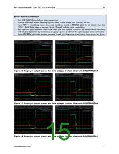
The MOSFETs offer roughly 20ns slope time at the lowest driver strength setting. Switching quality is
good and signals are clean (Figure 3.6, ff.). At double drive strength, the slope time halves, and
switching events still are clean. When increasing to full gate drive strength faster slopes lead to
increased ringing on all signals. Low or medium slope setting is best. Additional gate resistors or 1nF
output capacitors do not bring any additional improvement. The layout already proves to be good.
No additional components were required!
+VM
VS
LOW-
ESR
220nF
4.7µF
CV
HSV
V
CB
HS
LS
RG
Coil
out
RS
VSENSE
LSV
RP
RG
Additional 1A type Schottky Diodes (20V type sufficient) in
combination with high resistance gate resistors >10Ohm
Figure 3.9 Diodes for safe off condition with high gate series resistance
BRIDGE LAYOUT CONSIDERATIONS
-
-
Tune the bridge layout for minimum loop inductivity. A compact layout is best.
Keep MOSFET gate connections short and straight and avoid loop inductivity between bridge
feedback (U,V,W) and corresponding HS driver pin. Loop inductance is minimized with parallel
traces, or adjacent traces on adjacent layers. A wider trace reduces inductivity (don’t use minimum
trace width).
-
Place the TMC6200 near the low side MOSFETs GND connections, with its GND connections directly
connected to the same GND plane.
-
-
-
Optimize switching behavior by using lowest acceptable gate current setting.
Check influence of optional components shown in Figure 3.5.
Measure the performance of the bridge by probing BM pins directly at the bridge or at the
TMC6200 using a short GND tip on the scope probe rather than a GND cable, if available.
www.trinamic.com

 TRINAMIC [ TRINAMIC MOTION CONTROL GMBH & CO. KG. ]