TMC4361 DATASHEET (Rev. 2.68 / 2015-Apr-14) Preliminary
12
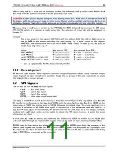
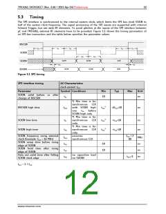
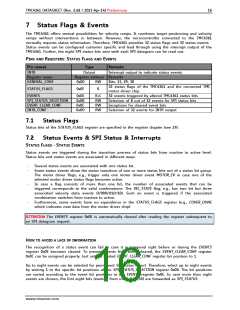
5.3 Timing
The SPI interface is synchronized to the internal system clock, which limits the SPI bus clock SCKIN to
half of the system clock frequency. The signal processing of the SPI inputs are supported with internal
Schmitt Trigger, but not with RC elements. To avoid glitches at the inputs of the SPI interface between
µC and TMC4361, external RC elements have to be provided. Figure 5.1 shows the timing parameters of
an SPI bus transaction and the table below specifies the parameter values.
NSCSIN
tCC
tCL
tCH
tCH
tCC
SCKIN
SDIIN
SDOIN
tDU
tDH
bit39
bit38
bit0
bit0
tDO
tZC
bit39
bit38
Figure 5.1 SPI timing
SPI interface timing
Parameter
AC-Characteristics
clock period: tCLK
Symbol Conditions
Min
Typ
Max
Unit
SCKIN valid before or after
change of NSCSIN
tCC
10
ns
*) Min time is for
synchronous CLK
with SCKIN high
*)
NSCSIN high time
tCSH
tCLK
>2tCLK+10
ns
one
tCH
before
SCSIN high only
*) Min time is for
synchronous CLK
only
*) Min time is for
synchronous CLK
only
*)
SCKIN low time
SCKIN high time
tCL
tCLK
>tCLK+10
>tCLK+10
ns
ns
*)
tCH
tCLK
SCKIN frequency using external
clock (Example: fCLK = 16 MHz)
SDIIN setup time before rising
edge of SCKIN
SDIIN hold time after rising
edge of SCKIN
assumes
synchronous CLK
fCLK / 2
(8)
fSCK
tDU
tDH
tDO
MHz
ns
10
10
ns
Data out valid time after falling
SCKIN clock edge
no capacitive load
on SDOIN
tFILT+5
ns
tCLK = 1 / fCLK
www.trinamic.com

 TRINAMIC [ TRINAMIC MOTION CONTROL GMBH & CO. KG. ]