UCD90320
www.ti.com.cn
ZHCSFI3B –AUGUST 2016–REVISED MAY 2019
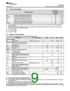
7.4 Thermal Information
UCD90320
THERMAL METRIC(1)
ZWS (BGA)
169 PINS
41.6
UNIT
RθJA
Junction-to-ambient thermal resistance(2)(3)
Junction-to-case (top) thermal resistance(2)
Junction-to-board thermal resistance(2)(4)(5)
Junction-to-top characterization parameter(6)
Junction-to-board characterization parameter(4)
Junction-to-case (bottom) thermal resistance
°C/W
°C/W
°C/W
°C/W
°C/W
°C/W
RθJC(top)
RθJB
15.8
18.9
ψJT
0.3
ψJB
20.3
RθJC(bot)
n/a
(1) For more information about traditional and new thermal metrics, see the Semiconductor and IC Package Thermal Metrics application
report, SPRA953.
(2) Junction to ambient thermal resistance (θJA), junction to board thermal resistance (θJB), and junction to case thermal resistance (θJC
)
numbers are determined by a package simulator.
(3) TJ = TA + (P × θJA
)
(4) TJ = TPCB + (P × ΨJB
)
()
(5) TJ = TB + (P × θJB
)
(6) TJ = TC + (P × ΨJT
)
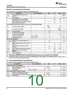
7.5 Electrical Characteristics
over operating free-air temperature range (unless otherwise noted)
PARAMETER
TEST CONDITIONS
MIN
TYP
MAX
UNIT
SUPPLY CURRENT
IV33 Supply Current
VV33D = VV33A = 3.3 V
31.4
54.9
mA
ON-CHIP LOW DROP-OUT (LDO) REGULATOR
External filter capacitor size for internal
CLDO
2.5
4
µF
power supply(1)
VLDO
LDO output voltage
Inrush current
1.08
50
1.2
1.32
250
V
IINRUSH
mA
ANALOG-TO-DIGITAL CONVERTER (ADC)(2)(3)
V33A
AVSS
ADC supply voltage
ADC ground voltage
2.97
3.3
0
3.63
V
V
Voltage reference decoupling capacitance
between V33A and AVSS (if using internal
reference)
CV33A
1.01
µF
V
(4)
Positive external voltage reference on
VREFA+ pin
VREFA+
2.4
3
Negative external voltage reference on
VREF– pin
VREF–
IREF
VAVSS
AVSS
330.5
0.3
V
Current on VREF+ pin input
External VREF+ = 3.3 V
440
µA
Voltage reference decoupling capacitance
between VREFA+ and VREFA– (if using
external reference)(4)
Analog input range, internal reference(5)
Analog input range, external reference(6)
ADC input leakage current
CREF
1.01
µF
V
0
V33A
VVREFA+
2
VADCIN
VVREFA–
IL
µA
kΩ
pF
RADC
CADC
ADC equivalent input resistance
ADC equivalent input capacitance
2.5
10
(1) Connect the capacitor as close as possible to pin D6.
(2) Total of two ADC channels run independently during normal operation.
(3) Total unadjusted error is the maximum error at any one code versus the ideal ADC curve. It includes offset error, gain error, and INL at
any given ADC code.
(4) Two capacitors (1.0 µF and 0.01 µF) connected in parallel.
(5) Internal reference is connected directly between V33A and AVSS.
(6) External reference noise level must be under 12 bit (–74 dB) of full scale input, over input bandwidth, measured at VREFA+ - VREFA–.
Copyright © 2016–2019, Texas Instruments Incorporated
9

 TI [ TEXAS INSTRUMENTS ]