UCD90320
ZHCSFI3B –AUGUST 2016–REVISED MAY 2019
www.ti.com.cn
7 Specifications
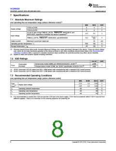
7.1 Absolute Maximum Ratings
over operating free-air temperature range (unless otherwise noted)(1)
MIN
0
MAX
UNIT
V
V33D to DVSS
Supply voltage
4
4
V33A to AVSS
0
V
on all I/O pins except PMBUS_CNTRL, PMBALERT, MARGIN19, and
–0.3
–0.3
5.5
V
V
MARGIN20, regardless of whether the device is powered(2)
PMBUS_CNTRL, PMBALERT, MARGIN19, and MARGIN20
Maximum current per output pin
Input voltage
VV33D
0.3
+
Output current
25
mA
°C
Operating junction temperature, TJ
Storage temperature, Tstg
TBD
–65
150
150
°C
(1) Stresses beyond those listed under Absolute Maximum Ratings may cause permanent damage to the device. These are stress ratings
only, which do not imply functional operation of the device at these or any other conditions beyond those listed in the Recommended
Operating Conditions table. Exposure to absolute-maximum-rated conditions for extended periods may affect device reliability.
(2) Applies to static and dynamic signals including overshoot.
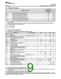
7.2 ESD Ratings
VALUE
±2000
±500
UNIT
Human-body model (HBM), per ANSI/ESDA/JEDEC JS-001(1)
Charged-device model (CDM), per JEDEC specification JESD22-C101(2)
Electrostatic
discharge
V(ESD)
V
(1) JEDEC document JEP155 states that 500-V HBM allows safe manufacturing with a standard ESD control process.
(2) JEDEC document JEP157 states that 250-V CDM allows safe manufacturing with a standard ESD control process.
7.3 Recommended Operating Conditions
over operating free-air temperature range (unless otherwise noted)
MIN
3.15
2.97
–40
–40
–40
NOM
3.3
MAX
3.63
3.63
85
UNIT
V
VV33D
VV33A
TA
Supply input voltage
(1)
3.3
V
Operating ambient temperature
Operating case temperature
Operating junction temperature
°C
°C
°C
TC
90
TJ
93
(1) It is recommended to connect the V33A pin and the V33D pin to the same supply. V33A must be powered before V33D if sourced from
different supplies. There is no restriction on the ordering sequence for powering off.
8
Copyright © 2016–2019, Texas Instruments Incorporated

 TI [ TEXAS INSTRUMENTS ]