UCD90320
ZHCSFI3B –AUGUST 2016–REVISED MAY 2019
www.ti.com.cn
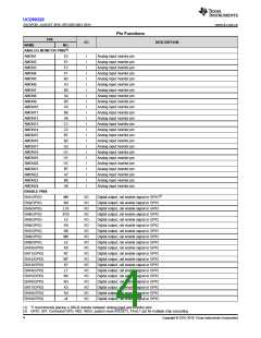
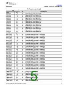
Pin Functions (continued)
PIN
I/O
DESCRIPTION
NAME
NO.
DMON8(GPIO)
GPIO
M11
I/O
Digital input monitor pin or GPIO
GPIO1
B11
B12
C11
A12
K2
I/O
I/O
I/O
I/O
I/O
GPIO
GPIO2
GPIO
GPIO3
GPIO
GPIO4
GPIO
SYNC_CLK
Synchronization clock I/O for multiple chip cascading
LOGIC GPO PINS
LGPO1(GPIO)
LGPO2(GPIO)
LGPO3(GPIO)
LGPO4(GPIO)
LGPO5(GPIO)
LGPO6(GPIO)
LGPO7(GPIO)
LGPO8(GPIO)
LGPO9(GPIO)
LGPO10(GPIO)
LGPO11(GPIO)
LGPO12(GPIO)
LGPO13(GPIO)
LGPO14(GPIO)
LGPO15(GPIO)
LGPO16(GPIO)
C9
B9
A9
C8
D5
C5
C6
C4
L3
I/O
I/O
I/O
I/O
I/O
I/O
I/O
I/O
I/O
I/O
I/O
I/O
I/O
I/O
I/O
I/O
Logic GPO or GPIO
Logic GPO or GPIO
Logic GPO or GPIO
Logic GPO or GPIO
Logic GPO or GPIO
Logic GPO or GPIO
Logic GPO or GPIO
Logic GPO or GPIO
Logic GPO or GPIO
Logic GPO or GPIO
Logic GPO or GPIO
Logic GPO or GPIO
Logic GPO or GPIO
Logic GPO or GPIO
Logic GPO or GPIO
Logic GPO or GPIO
M1
M2
M3
L4
N1
M4
N2
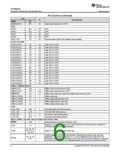
PMBus COMM INTERFACE
PMBUS_CLK
PMBUS_DATA
PMBALERT
PMBUS_CNTRL
PMBUS_ADDR0
PMBUS_ADDR1
PMBUS_ADDR2
JTAG
E10
D13
F11
E11
L2
I
PMBus clock (must pull up to V33D)
PMBus data (must pull up to V33D)
PMBus alert, active-low, open-drain output (must pull up to V33D)
PMBus control pin
I/O
O
I
I
PMBus digital address input. Bit 0
PMBus digital address input. Bit 1
PMBus digital address input. Bit 2
L1
I
K1
I
JTAG_TMS
A10
C10
A11
B10
I
I
Test mode select with internal pull-up
Test clock with internal pull-up
Test data out with internal pull-up
Test data in with internal pull-up
JTAG_TCK
JTAG_TDO
O
I
JTAG_TDI
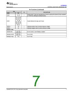
INPUT POWER, GROUND, AND EXTERNAL REFERENCE PINS
RESET
G10
I
Active-low device reset input. Pull up to V33D.
Analog 3.3-V supply. Decouple from V33D to minimize the electrical noise contained on
V33D from affecting the analog functions.
V33A
D3
I
D7, E6, E8,
E9, F10, J7,
J9, J10
V33D
I
I
Digital 3.3-V supply for I/O and some logic.
Positive supply for most of the logic function, including the processor core and most
peripherals. The voltage on this pin is 1.2 V and is supplied by the on-chip LDO. The
BPCap pins should only be connected to each other and an external capacitor as specified
in On-Chip Low Drop-Out (LDO) Regulator section of the Electrical Characteristics table.
D6, J1, J6,
K13
BPCap
6
Copyright © 2016–2019, Texas Instruments Incorporated

 TI [ TEXAS INSTRUMENTS ]