UCD90320
www.ti.com.cn
ZHCSFI3B –AUGUST 2016–REVISED MAY 2019
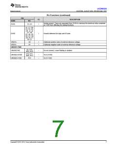
Pin Functions (continued)
PIN
I/O
DESCRIPTION
NAME
NO.
Analog ground. These are separated from DVSS to minimize the electrical noise contained
on V33D from affecting the analog functions.
AVSS
C3, E3
I
A1, C7, D9,
E5, F9, H5,
H9, J5, J8,
J11, H6,
H7, H8, G5,
G6, G7, G8,
G9, F6, F7,
F8, E7
DVSS
I
Ground reference for logic and I/O pins.
VREFA+
VREFA-
D2
D1
I
I
(Optional) positive node of external reference voltage
(Optional) negative node of external reference voltage
UNUSED PINS
A2, G13,
M12, N10
UNUSED-NC
–
Do not connect. Leave floating or isolated.
G12, K11,
M10, N13
UNUSED-DVSS
UNUSED-V33D
–
–
Tie to DVSS.
Tie to V33D.
K12
Copyright © 2016–2019, Texas Instruments Incorporated
7

 TI [ TEXAS INSTRUMENTS ]