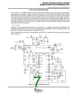
ꢀꢁꢁ ꢂ ꢃꢄ ꢅ ꢆ ꢀꢁꢁ ꢂ ꢃꢄ ꢃ ꢆ ꢀꢁꢁ ꢇ ꢃꢄ ꢅ ꢆ ꢀ ꢁꢁ ꢇꢃ ꢄꢃ
ꢈꢉ ꢁꢊꢋ ꢌ ꢍꢋ ꢎ ꢏꢐ ꢑꢒꢁꢓꢋ ꢐ ꢍꢐ ꢏꢐꢏꢔ ꢀꢕ ꢒꢓꢋ ꢐ
ꢖ
SLUS395J - FEBRUARY 2000 - REVISED MARCH 2009
APPLICATION INFORMATION
Conduction loss is calculated as the product of the R
and the square of RMS current:
of the switch (at the worst case junction temperature)
DS(on)
2
P
+ R
K I
COND
DS(on)
RMS
where K is the temperature factor found in the manufacturer’s R
vs. junction temperature curves.
DS(on)
Calculating these losses and plotting against frequency gives a curve that enables the designer to determine
either which manufacturer’s device has the best performance at the desired switching frequency, or which
switching frequency has the least total loss for a particular power switch. For this design example an IRFP450
HEXFET from International Rectifier was chosen because of its low R
and its V
rating. The IRFP450’s
DS(on)
DSS
R
of 0.4 Ω and the maximum V
of 500 V made it an ideal choice. An excellent review of this procedure
DS(on)
DSS
can be found in the Unitrode Power Supply Design Seminar SEM1200, Topic 6, Design Review: 140 W, [Multiple
Output High Density DC/DC Converter].
softstart
The softstart circuitry is used to prevent overshoot of the output voltage during start up. This is accomplished
by bringing up the voltage amplifier’s output (V ) slowly which allows for the PWM duty cycle to increase
VAOUT
slowly. Please use the following equation to select a capacitor for the softstart pin.
In this example t is equal to 7.5 ms, which would yield a C of 10 nF.
DELAY
SS
10 mA t
DELAY
7.5 V
C
+
SS
In an open-loop test circuit, shorting the softstart pin to ground does not ensure 0% duty cycle. This is due to
the current amplifiers input offset voltage, which could force the current amplifier output high or low depending
on the polarity of the offset voltage. However, in the typical application there is sufficient amount of inrush and
bias current to overcome the current amplifier’s offset voltage.
multiplier
The output of the multiplier of the UCC3817 is a signal representing the desired input line current. It is an input
to the current amplifier, which programs the current loop to control the input current to give high power factor
operation. As such, the proper functioning of the multiplier is key to the success of the design. The inputs to the
multiplier are VAOUT, the voltage amplifier error signal, I
, a representation of the input rectified ac line
IAC
voltage, and an input voltage feedforward signal, V
as:
. The output of the multiplier, I
, can be expressed
VFF
MOUT
ǒVVAOUT * 1Ǔ
I
+ I
MOUT
IAC
2
K V
VFF
1
V
where K is a constant typically equal to
.
The electrical characteristics table covers all the required operating conditions for designing with the
multiplier. Additionally, curves in figures 10, 11, and 12 provide typical multiplier characteristics over its entire
operating range.
9
www.ti.com

 TI [ TEXAS INSTRUMENTS ]