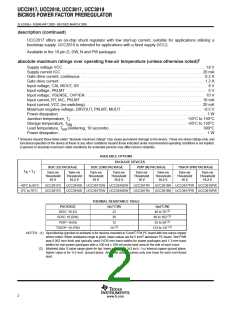
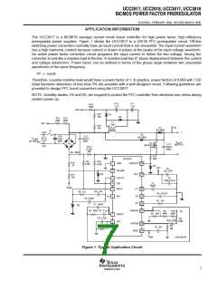
ꢀ ꢁꢁꢂ ꢃ ꢄ ꢅ ꢆ ꢀ ꢁꢁ ꢂ ꢃꢄ ꢃ ꢆ ꢀꢁ ꢁꢇ ꢃ ꢄ ꢅ ꢆ ꢀꢁ ꢁꢇ ꢃ ꢄ ꢃ
ꢈ ꢉꢁꢊ ꢋꢌ ꢍꢋꢎ ꢏꢐ ꢑꢒꢁ ꢓꢋ ꢐ ꢍ ꢐꢏ ꢐꢏ ꢔꢀ ꢕꢒꢓꢋ ꢐ
ꢖ
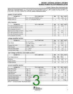
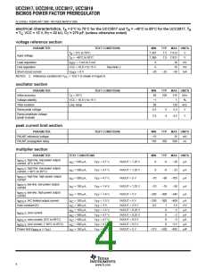
SLUS395J - FEBRUARY 2000 - REVISED MARCH 2009
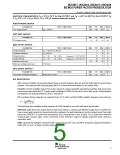
pin descriptions (continued)
IAC: (current proportional to input voltage) This input to the analog multiplier is a current proportional to
instantaneous line voltage. The multiplier is tailored for very low distortion from this current input (I ) to
IAC
multiplier output. The recommended maximum I
is 500 µA.
IAC
MOUT: (multiplier output and current amplifier inverting input) The output of the analog multiplier and the
inverting input of the current amplifier are connected together at MOUT. As the multiplier output is a current, this
is a high-impedance input so the amplifier can be configured as a differential amplifier. This configuration
improves noise immunity and allows for the leading-edge modulation operation. The multiplier output current
is limited to ǒ2 I Ǔ. The multiplier output current is given by the equation:
IAC
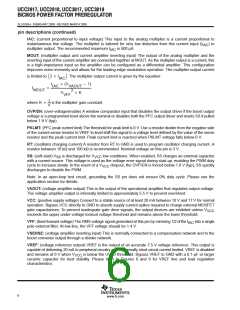
I
(V
* 1)
IAC
VAOUT
I
+
MOUT
2
V
K
VFF
1
V
where K + is the multiplier gain constant.
OVP/EN: (over-voltage/enable) A window comparator input that disables the output driver if the boost output
voltage is a programmed level above the nominal or disables both the PFC output driver and resets SS if pulled
below 1.9 V (typ).
PKLMT: (PFC peak current limit) The threshold for peak limit is 0 V. Use a resistor divider from the negative side
of the current sense resistor to VREF to level shift this signal to a voltage level defined by the value of the sense
resistor and the peak current limit. Peak current limit is reached when PKLMT voltage falls below 0 V.
RT: (oscillator charging current) A resistor from RT to GND is used to program oscillator charging current. A
resistor between 10 kΩ and 100 kΩ is recommended. Nominal voltage on this pin is 3 V.
SS: (soft-start) V is discharged for V
with a current source. This voltage is used as the voltage error signal during start-up, enabling the PWM duty
low conditions. When enabled, SS charges an external capacitor
SS
VCC
cycle to increase slowly. In the event of a V
discharges to disable the PWM.
dropout, the OVP/EN is forced below 1.9 V (typ), SS quickly
VCC
Note: In an open-loop test circuit, grounding the SS pin does not ensure 0% duty cycle. Please see the
application section for details.
VAOUT: (voltage amplifier output) This is the output of the operational amplifier that regulates output voltage.
The voltage amplifier output is internally limited to approximately 5.5 V to prevent overshoot.
VCC: (positive supply voltage) Connect to a stable source of at least 20 mA between 10 V and 17 V for normal
operation. Bypass VCC directly to GND to absorb supply current spikes required to charge external MOSFET
gate capacitances. To prevent inadequate gate drive signals, the output devices are inhibited unless V
exceeds the upper under-voltage lockout voltage threshold and remains above the lower threshold.
VCC
VFF: (feed-forward voltage) The RMS voltage signal generated at this pin by mirroring 1/2 of the I
pole external filter. At low line, the VFF voltage should be 1.4 V.
into a single
IAC
VSENSE: (voltage amplifier inverting input) This is normally connected to a compensation network and to the
boost converter output through a divider network.
VREF: (voltage reference output) VREF is the output of an accurate 7.5-V voltage reference. This output is
capable of delivering 20 mA to peripheral circuitry and is internally short-circuit current limited. VREF is disabled
and remains at 0 V when V
is below the UVLO threshold. Bypass VREF to GND with a 0.1-µF or larger
VCC
ceramic capacitor for best stability. Please refer to Figures 8 and 9 for VREF line and load regulation
characteristics.
6
www.ti.com

 TI [ TEXAS INSTRUMENTS ]