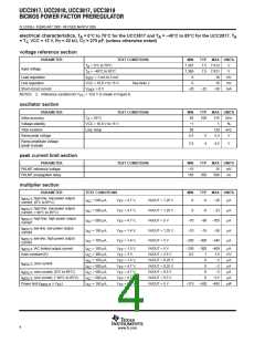
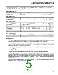
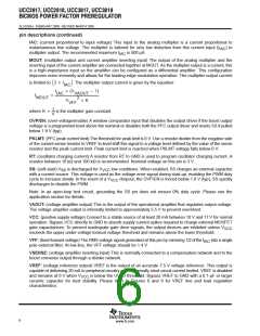
ꢀ ꢁꢁꢂ ꢃ ꢄ ꢅ ꢆ ꢀ ꢁꢁ ꢂ ꢃꢄ ꢃ ꢆ ꢀꢁ ꢁꢇ ꢃ ꢄ ꢅ ꢆ ꢀꢁ ꢁꢇ ꢃ ꢄ ꢃ
ꢈ ꢉꢁꢊ ꢋꢌ ꢍꢋꢎ ꢏꢐ ꢑꢒꢁ ꢓꢋ ꢐ ꢍ ꢐꢏ ꢐꢏ ꢔꢀ ꢕꢒꢓꢋ ꢐ
ꢖ
SLUS395J - FEBRUARY 2000 - REVISED MARCH 2009
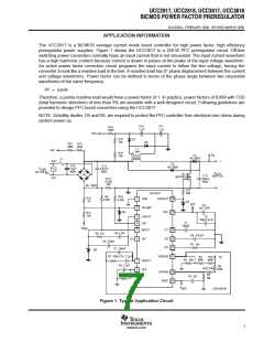
APPLICATION INFORMATION
power stage
L
: The boost inductor value is determined by:
BOOST
ǒVIN(min) DǓ
+
L
BOOST
(
)
DI fs
where D is the duty cycle, ∆I is the inductor ripple current and f is the switching frequency. For the example
S
circuit a switching frequency of 100 kHz, a ripple current of 875 mA, a maximum duty cycle of 0.688 and a
minimum input voltage of 85 V
equation are at the peak of low line, where the inductor current and its ripple are at a maximum.
gives us a boost inductor value of about 1 mH. The values used in this
RMS
C
: Two main criteria, the capacitance and the voltage rating, dictate the selection of the output capacitor.
OUT
The value of capacitance is determined by the holdup time required for supporting the load after input ac voltage
is removed. Holdup is the amount of time that the output stays in regulation after the input has been removed.
For this circuit, the desired holdup time is approximately 16 ms. Expressing the capacitor value in terms of output
power, output voltage, and holdup time gives the equation:
ǒ2 P DtǓ
OUT
C
+ ǒV
OUT(min) Ǔ
OUT
2
2
* V
OUT
In practice, the calculated minimum capacitor value may be inadequate because output ripple voltage
specifications limit the amount of allowable output capacitor ESR. Attaining a sufficiently low value of ESR often
necessitates the use of a much larger capacitor value than calculated. The amount of output capacitor ESR
allowed can be determined by dividing the maximum specified output ripple voltage by the inductor ripple
current. In this design holdup time was the dominant determining factor and a 220-µF, 450-V capacitor was
chosen for the output voltage level of 385 VDC at 250 W.
Power switch selection: As in any power supply design, tradeoffs between performance, cost and size have
to be made. When selecting a power switch, it can be useful to calculate the total power dissipation in the switch
for several different devices at the switching frequencies being considered for the converter. Total power
dissipation in the switch is the sum of switching loss and conduction loss. Switching losses are the combination
of the gate charge loss, C
loss and turnon and turnoff losses:
OSS
P
P
P
+ Q
V
fs
GATE
COSS
GATE
GATE
1
2
2
+
C
V
fs
OSS
OFF
1
2
I ǒtON
Ǔ
) P
+
V
) t
fs
ON
OFF
OFF
L
OFF
where Q
is the total gate charge, V
is the gate drive voltage, f is the clock frequency, C
is the drain
OSS
GATE
GATE
L
S
source capacitance of the MOSFET, I is the peak inductor current, t
(estimated using device parameters R
off time, in this case V
and t
are the switching times
ON
OFF
, Q
and V ) and V
is the voltage across the switch during the
GATE GD
TH
OFF
= V
.
OFF
OUT
8
www.ti.com

 TI [ TEXAS INSTRUMENTS ]