ꢀꢁꢁ ꢂ ꢃꢄ ꢅ ꢆ ꢀꢁꢁ ꢂ ꢃꢄ ꢃ ꢆ ꢀꢁꢁ ꢇ ꢃꢄ ꢅ ꢆ ꢀ ꢁꢁ ꢇꢃ ꢄꢃ
ꢈꢉ ꢁꢊꢋ ꢌ ꢍꢋ ꢎ ꢏꢐ ꢑꢒꢁꢓꢋ ꢐ ꢍꢐ ꢏꢐꢏꢔ ꢀꢕ ꢒꢓꢋ ꢐ
ꢖ
SLUS395J - FEBRUARY 2000 - REVISED MARCH 2009
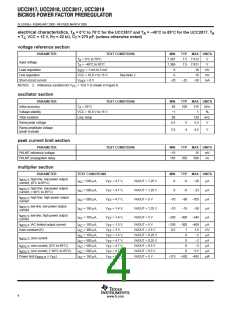
electrical characteristics, T = 0°C to 70°C for the UCC3817 and T = −40°C to 85°C for the UCC2817, T
A
T
A
A
= T VCC = 12 V, R = 22 kΩ, C = 270 pF, (unless otherwise noted)
J,
T
feed-forward section
PARAMETER
TEST CONDITIONS
TEST CONDITIONS
TEST CONDITIONS
MIN
TYP
MAX UNITS
µA
VFF output current
I
= 300 µA
−140 −150 −160
AC
soft start section
PARAMETER
MIN
TYP
MAX UNITS
−16 µA
SS charge current
−6
−10
gate driver section
PARAMETER
Pullup resistance
MIN
TYP
5
MAX UNITS
I
I
= –100 mA to −200 mA
= 100 mA
12
10
50
50
99
2
Ω
Ω
O
Pulldown resistance
Output rise time
2
O
C
C
= 1 nF,
= 1 nF,
R
R
= 10 Ω,
= 10 Ω,
V
V
= 0.7 V to 9.0 V
= 9.0 V to 0.7 V
25
10
95
ns
ns
%
%
L
L
L
L
DRVOUT
Output fall time
DRVOUT
Maximum duty cycle
Minimum controlled duty cycle
93
At 100 kHz
zero power section
PARAMETER
TEST CONDITIONS
Measured on VAOUT
MIN
TYP
MAX UNITS
0.50
Zero power comparator threshold
0.20
0.33
V
pin descriptions
CAI: (current amplifier noninverting input) Place a resistor between this pin and the GND side of current sense
resistor. This input and the inverting input (MOUT) remain functional down to and below GND.
CAOUT: (current amplifier output) This is the output of a wide bandwidth operational amplifier that senses line
current and commands the PFC pulse-width modulator (PWM) to force the correct duty cycle. Compensation
components are placed between CAOUT and MOUT.
CT: (oscillator timing capacitor) A capacitor from CT to GND sets the PWM oscillator frequency according to:
0.6
RT CT
f [ ǒ
Ǔ
The lead from the oscillator timing capacitor to GND should be as short and direct as possible.
DRVOUT: (gate drive) The output drive for the boost switch is a totem-pole MOSFET gate driver on DRVOUT.
Use a series gate resistor to prevent interaction between the gate impedance and the output driver that might
cause the DRVOUT to overshoot excessively. See characteristic curve (Figure 13) to determine minimum
required gate resister value. Some overshoot of the DRVOUT output is always expected when driving a
capacitive load.
GND: (ground) All voltages measured with respect to ground. VCC and REF should be bypassed directly to
GND with a 0.1-µF or larger ceramic capacitor.
5
www.ti.com

 TI [ TEXAS INSTRUMENTS ]