ꢀ ꢁꢁꢂ ꢃ ꢄ ꢅ ꢆ ꢀ ꢁꢁ ꢂ ꢃꢄ ꢃ ꢆ ꢀꢁ ꢁꢇ ꢃ ꢄ ꢅ ꢆ ꢀꢁ ꢁꢇ ꢃ ꢄ ꢃ
ꢈ ꢉꢁꢊ ꢋꢌ ꢍꢋꢎ ꢏꢐ ꢑꢒꢁ ꢓꢋ ꢐ ꢍ ꢐꢏ ꢐꢏ ꢔꢀ ꢕꢒꢓꢋ ꢐ
ꢖ
SLUS395J - FEBRUARY 2000 - REVISED MARCH 2009
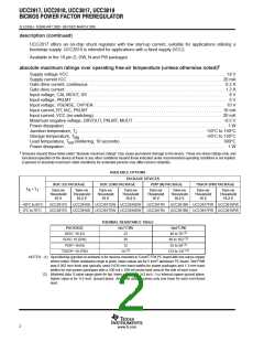
description (continued)
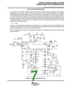
UCC2817 offers an on-chip shunt regulator with low start-up current, suitable for applications utilizing a
bootstrap supply. UCC2818 is intended for applications with a fixed supply (VCC).
Available in the 16-pin D, DW, N and PW packages.
†
absolute maximum ratings over operating free-air temperature (unless otherwise noted)
Supply voltage VCC . . . . . . . . . . . . . . . . . . . . . . . . . . . . . . . . . . . . . . . . . . . . . . . . . . . . . . . . . . . . . . . . . . . . . . . . 18 V
Supply current ICC . . . . . . . . . . . . . . . . . . . . . . . . . . . . . . . . . . . . . . . . . . . . . . . . . . . . . . . . . . . . . . . . . . . . . . . 20 mA
Gate drive current, continuous . . . . . . . . . . . . . . . . . . . . . . . . . . . . . . . . . . . . . . . . . . . . . . . . . . . . . . . . . . . . . . 0.2 A
Gate drive current . . . . . . . . . . . . . . . . . . . . . . . . . . . . . . . . . . . . . . . . . . . . . . . . . . . . . . . . . . . . . . . . . . . . . . . . . 1.2 A
Input voltage, CAI, MOUT, SS . . . . . . . . . . . . . . . . . . . . . . . . . . . . . . . . . . . . . . . . . . . . . . . . . . . . . . . . . . . . . . . . . 8 V
Input voltage, PKLMT . . . . . . . . . . . . . . . . . . . . . . . . . . . . . . . . . . . . . . . . . . . . . . . . . . . . . . . . . . . . . . . . . . . . . . . . 5 V
Input voltage, VSENSE, OVP/EN . . . . . . . . . . . . . . . . . . . . . . . . . . . . . . . . . . . . . . . . . . . . . . . . . . . . . . . . . . . . . 10 V
Input current, RT, IAC, PKLMT . . . . . . . . . . . . . . . . . . . . . . . . . . . . . . . . . . . . . . . . . . . . . . . . . . . . . . . . . . . . . 10 mA
Input current, VCC (no switching) . . . . . . . . . . . . . . . . . . . . . . . . . . . . . . . . . . . . . . . . . . . . . . . . . . . . . . . . . . . 20 mA
Maximum negative voltage, DRVOUT, PKLMT, MOUT . . . . . . . . . . . . . . . . . . . . . . . . . . . . . . . . . . . . . . . . −0.5 V
Power dissipation . . . . . . . . . . . . . . . . . . . . . . . . . . . . . . . . . . . . . . . . . . . . . . . . . . . . . . . . . . . . . . . . . . . . . . . . . . . 1 W
Junction temperature, T . . . . . . . . . . . . . . . . . . . . . . . . . . . . . . . . . . . . . . . . . . . . . . . . . . . . . . . . . . −55°C to 150°C
J
stg
Storage temperature, T
. . . . . . . . . . . . . . . . . . . . . . . . . . . . . . . . . . . . . . . . . . . . . . . . . . . . . . . . . −65°C to 150°C
Lead temperature, T (soldering, 10 seconds) . . . . . . . . . . . . . . . . . . . . . . . . . . . . . . . . . . . . . . . . . . . . . . . 300°C
Power dissipation . . . . . . . . . . . . . . . . . . . . . . . . . . . . . . . . . . . . . . . . . . . . . . . . . . . . . . . . . . . . . . . . . . . . . . . . . . . 1 W
sol
†
Stresses beyond those listed under “absolute maximum ratings” may cause permanent damage to the device. These are stress ratings only, and
functional operation of the device at these or any other conditions beyond those indicated under recommended operating conditions is not implied.
Exposure to absolute-maximum-rated conditions for extended periods may affect device reliability.
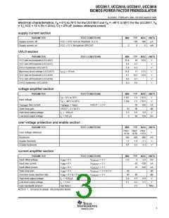
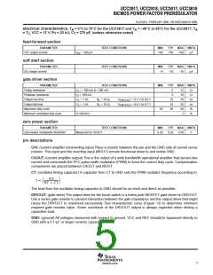
AVAILABLE OPTIONS
PACKAGE DEVICES
SOIC (D) PACKAGE
SOIC (DW) PACKAGE
PDIP (N) PACKAGE
TSSOP (PW) PACKAGE
T
A
= T
J
Turn-on
Threshold
16 V
Turn-on
Threshold
10.2 V
Turn-on
Threshold
16 V
Turn-on
Threshold
10.2 V
Turn-on
Threshold
16 V
Turn-on
Threshold
10.2 V
Turn-on
Threshold
16 V
Turn-on
Threshold
10.2 V
−40°C to 85°C
0°C to 70°C
UCC2817D
UCC3817D
UCC2818D UCC2817DW UCC2818DW
UCC3818D UCC3817DW UCC3818DW
UCC2817N
UCC3817N
UCC2818N UCC2817PW UCC2818PW
UCC3818N UCC3817PW UCC3818PW
THERMAL RESISTANCE TABLE
PACKAGE
θjc(°C/W)
θja(°C/W)
(1)
(1)
(1)
SOIC−16 (D)
SOIC−16 (DW)
PDIP−16 (N)
22
26
12
40 to 70
89 to 102
25 to 50
(2)
(2)
TSSOP−16 (PW)
14
123 to 147
2
NOTES: (1) Specifiedθja (junction to ambient) is for devices mounted to 5-inch FR4 PC board with one ounce copper
2
where noted. When resistance range is given, lower values are for 5 inch aluminum PC board. Test PWB
was 0.062 inch thick and typically used 0.635-mm trace widths for power packages and 1.3-mm trace
widths for non-power packages with a 100-mil x 100-mil probe land area at the end of each trace.
(2). Modeled data. If value range given for θja, lower value is for 3x3 inch. 1 oz internal copper ground plane,
higher value is for 1x1-inch. ground plane. All model data assumes only one trace for each non-fused
lead.
2
www.ti.com

 TI [ TEXAS INSTRUMENTS ]