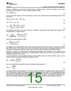
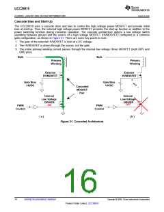
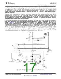
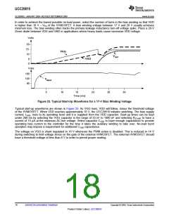
UCC28610
www.ti.com ......................................................................................................................................... SLUS888C–JANUARY 2009–REVISED SEPTEMBER 2009
Feedback Function
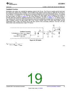
Modulation and modes are controlled by applying current to the FB pin. The FB pin is usually used to feed back
the output error signal to the modulator. The UCC28610 uses internal current mirrors to apply the FB current to
the Feedback Processing block, and then to the Frequency Modulator and Current Modulator blocks. The voltage
of the FB pin is a constant 0.7 V. AC filtering of the output of the opto-coupler must be applied to the emitter of
the opto-coupler, as shown in Figure 24. The corner frequency of the filter in Figure 24 should be at least a
decade above the maximum switching frequency of the converter, as given in Equation 11. A 100-kΩ resistor,
RFB, between the FB pin and GND prevents ground noise from resetting the overload timer by biasing the FB pin
with a negative current. An opto-coupler with a low Current Transfer Ratio (CTR) often gives better no-load
performance than a high CTR device due to the bias current of the secondary reference. The low CTR also
offers better noise immunity than a high CTR device.
VDD
IFB
RFB filter
FeedBack Processing
IFB
1
To Modulators
0uA < IFB < 200uA
IFB > 200uA
IFB = 0A
FB
RFB
CFBfilter
GM
OverLoad
Figure 24. FB Details
1
fFB
=
2´p ´RFBfilter ´CFBfilter
(11)
Copyright © 2009, Texas Instruments Incorporated
Submit Documentation Feedback
19
Product Folder Link(s): UCC28610

 TI [ TEXAS INSTRUMENTS ]