UCC28610
www.ti.com ......................................................................................................................................... SLUS888C–JANUARY 2009–REVISED SEPTEMBER 2009
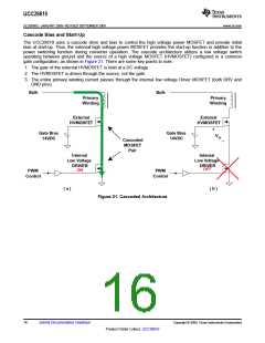
The UCC28610 integrates the low voltage switch in the form of a 90-mΩ FET along with all associated current
sensing and drive. The HVMOSFET is forced to track the fast internal low voltage driver. The drain-gate charge
in the HVMOSFET does not affect the turn-off speed because the gate is connected to a low impedance DC
source. The cascode configuration results in very fast turn-off of the HVMOSFET, which keeps MOSFET
switching losses low.
Cascode drive circuits are well known for high speed voltage gain. This topology can have small signal
bandwidth over 100 MHz and it can exhibit high frequency ringing. High frequency ringing can cause EMI
problems and become destructive in some situations. The sub-intervals during and immediately following the
turn-on and turn-off transients are particularly susceptible to oscillation. For avoidance or solutions, see the
application section, Solving High Frequency Ringing.
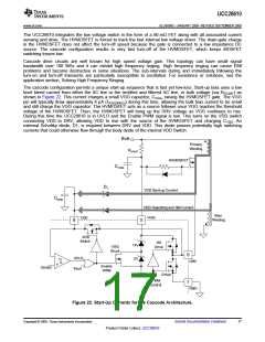
The cascode configuration permits a unique start-up sequence that is fast yet low-loss. Start-up bias uses a low
level bleed current from either the AC line or the rectified and filtered AC line, or bulk voltage (via RSTART) as
shown in Figure 22. This current charges a small VGG capacitor, CVGG, raising the HVMOSFET gate. The VGG
pin will typically draw approximately 6 µA (IVGG(SREG)) during this time, allowing the bulk bias current to be small
and still charge the VGG capacitor. The HVMOSFET acts as a source follower once VGG reaches the threshold
voltage of the HVMOSFET. Then, the HVMOSFET will bring up the DRV voltage as VGG continues to rise.
During this time the UCC28610 is in UVLO and the Enable PWM signal is low. This turns on the VDD switch
connecting VDD to DRV, allowing VDD to rise with the source of the HVMOSFET and charging CVDD. An
external Schottky diode, D1, is required between DRV and VDD. This diode passes potentially high switching
currents that could otherwise flow through the body diode of the internal VDD Switch.
Bulk
Primary
Winding
RSTART
HVMOSFET
CVGG
D1
VDD Start-up Current
CVDD
VDD Operating and GM Current
VGG
Bias
Winding
VDD
5
8
VDD
Switch
HS
Drive
14V
2V
VGG
Shunt
6
7
UVLO
DRV
+
Enable
PWM
10V/8V
Fault
Driver
PWM
Control
GND
Figure 22. Start-Up Currents for the Cascode Architecture.
Copyright © 2009, Texas Instruments Incorporated
Submit Documentation Feedback
17
Product Folder Link(s): UCC28610

 TI [ TEXAS INSTRUMENTS ]