UCC28951
www.ti.com.cn
ZHCSIQ7A –AUGUST 2018 –REVISED DECEMBER 2021
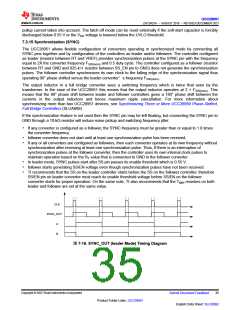
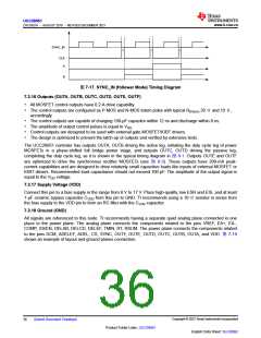
SYNC_IN
CLK
A
B
图7-17. SYNC_IN (follower Mode) Timing Diagram
7.3.16 Outputs (OUTA, OUTB, OUTC, OUTD, OUTE, OUTF)
• All MOSFET control outputs have 0.2-A drive capability.
• The control outputs are configured as P-MOS and N-MOS totem poles with typical RDS(on) 20 Ωand 10 Ω,
accordingly.
• The control outputs are capable of charging 100-pF capacitor within 12 ns and discharge within 8 ns.
• The amplitude of output control pulses is equal to VDD
.
• Control outputs are designed to be used with external gate MOSFET/IGBT drivers.
• The design is optimized to prevent the latch-up of outputs and verified by extensive tests.
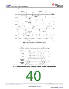
The UCC28951 controler has outputs OUTA, OUTB driving the active leg, initiating the duty cycle leg of power
MOSFETs in a phase-shifted full bridge power stage, and outputs OUTC, OUTD driving the passive leg,
completing the duty cycle leg, as it is shown in the typical timing diagram in 图 8-1. Outputs OUTE and OUTF
are optimized to drive the synchronous rectifier MOSFETs (see 图 8-3). These outputs have 200-mA peak-
current capabilities and are designed to drive relatively small capacitive loads like inputs of external MOSFET or
IGBT drivers. Recommended load capacitance should not exceed 100 pF. The amplitude of the output signal is
equal to the VDD voltage.
7.3.17 Supply Voltage (VDD)
Connect this pin to a bias supply in the range from 8 V to 17 V. Place high-quality, low ESR and ESL and at least
1-µF ceramic bypass capacitor CVDD from this pin to GND. TI recommends using a 10-Ω resistor in series from
the bias supply to the VDD pin to form an RC filter with the CVDD capacitor.
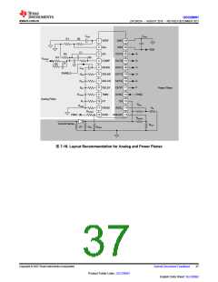
7.3.18 Ground (GND)
All signals are referenced to this node. TI recommends having a separate quiet analog plane connected in one
place to the power plane. The analog plane connects the components related to the pins VREF, EA+, EA-,
COMP, SS/EN, DELAB, DELCD, DELEF, TMIN, RT, RSUM. The power plane connects the components related
to the pins DCM, ADELEF, ADEL, CS, SYNC, OUTF, OUTE, OUTD, OUTC, OUTB, OUTA, and VDD. 图 7-18
shows an example of layout and ground planes connection.
Copyright © 2023 Texas Instruments Incorporated
English Data Sheet: SLUSDB2
36
Submit Document Feedback
Product Folder Links: UCC28951

 TI [ TEXAS INSTRUMENTS ]