UCC28951
www.ti.com.cn
ZHCSIQ7A –AUGUST 2018 –REVISED DECEMBER 2021
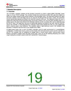
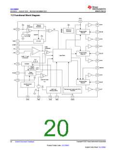
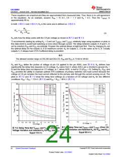
7.2 Functional Block Diagram
ADEL
14
VDD
VDD
22 OUTA
Thermal
UVLO
Shutdown
comparator
VDD 23
–
+
EN
Reference
Generator
Programmable
Delay AB
6
DELAB
+
–
ON/OFF
7.3-V Rise
6.7-V Fall
VDD
21 OUTB
20 OUTC
VREF
COMP
EA–
1
4
3
2
5-V LDO
PWM
comparator
–
+
–
+
+
EA+
Programmable
Delay CD
7
DELCD
Logic Block
Lower "+" Input
is Dominant
CLK
19 OUTD
13 ADELEF
18 OUTE
RT 10
Oscillator
RAMP
2.8 V
0.8 V
Ramp
Summing
RSUM 11
–
+
CS
Cycle-by-Cycle
ILIM
CS 15
Programmable
Delay EF
8
DELEF
Synchronization
Block
+
–
CS
Light-Load
Efficiency Block
Soft-start and Enable with 0.55-V
Threshold
17 OUTF
2 V
16
24
12
9
5
SYNC
GND
DCM
TMIN
SS/EN
Copyright © 2023 Texas Instruments Incorporated
English Data Sheet: SLUSDB2
20
Submit Document Feedback
Product Folder Links: UCC28951

 TI [ TEXAS INSTRUMENTS ]