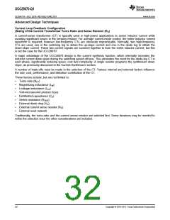
UCC28070-Q1
www.ti.com
SLUSA71A –JULY 2010–REVISED JUNE 2011
The switching ripple voltage should be attenuated to less than 1/10 of the ΔVRMP amplitude so as to be
considered "negligible" ripple.
Thus, CAOx gain at fPWM is:
DVRMP ´kSYNC
10
gmc Rzc £
RS
DILB ´
NCT
(23)
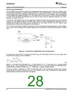
where ∆ILB is the maximum peak-to-peak ripple current in the boost inductor, and gmc is the transconductance of
the CA, 100 μS.
4V ´ NCT
Rzc £
10´100mS ´DILB ´ RS
(24)
The current-loop cross-over frequency is then found by equating the open loop gain to 1 and solving for fCXO
:
RS
Vout ´
NCT
fCXO
=
´ gmc Rzc
DVRMP ´kSYNC ´2p ´ LB
(25)
CCZ is then determined by setting fZC = fCXO = 1/(2πxRZCxCZC) and solving for CZC. At fZC = fCXO, a phase margin
of 45° is obtained at fCXO. Greater phase margin may be had by placing fZC < fCXO
.
An additional high-frequency pole is generally added at fPWM to further attenuate ripple and noise at fPWM and
higher. This is done by adding a small-value capacitor, Cpc, across the RzcCzc network.
1
Cpc =
2p ´ fPWM ´ Rzc
(26)
The procedure above is valid for fixed-value inductors.
NOTE
If a "swinging-choke" boost inductor (inductance decreases with increasing current) is
used, fCXO varies with inductance, so CZC should be determined at maximum inductance.
Copyright © 2010–2011, Texas Instruments Incorporated
29

 TI [ TEXAS INSTRUMENTS ]