UCC28070-Q1
www.ti.com
SLUSA71A –JULY 2010–REVISED JUNE 2011
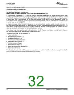
In general, 50 ≤ NCT ≤ 200 is a reasonable range from which to choose. If NCT is too low, there may be high
power loss in RS and insufficient LM. If too high, there could be excessive LLK and Cd. (A one-turn primary
winding is assumed.)
CSx
LLK
RSER
D
Reset
Network
IDS
1
NCT
LM iM
Cd
RS
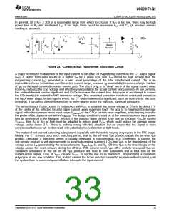
Figure 24. Current Sense Transformer Equivalent Circuit
A major contributor to distortion of the input current is the effect of magnetizing current on the CT output signal
(iRS). A higher turns-ratio results in a higher LM for a given core size. LM should be high enough that the
magnetizing current (iM) generated is a very small percentage of the total transformed current. This is an
impossible criterion to maintain over the entire current range, because iM unavoidably becomes a larger fraction
of iRS as the input current decreases toward zero. The effect of iM is to "steal" some of the signal current away
from RS, reducing the CSx voltage and effectively understating the actual current being sensed. At low currents,
this understatement can be significant and CAOx increases the current-loop duty-cycle in an attempt to correct
the CSx input(s) to match the IMO reference voltage. This unwanted correction results in overstated current on
the input wave shape in the regions where the CT understatement is significant, such as near the ac line zero
crossings. It can affect the entire waveform to some degree under the high line, light-load conditions.
The sense resistor RS is chosen, in conjunction with NCT, to establish the sense voltage at CSx to be about 3 V
at the center of the reflected inductor ripple current under maximum load. The goal is to maximize the average
signal within the common-mode input range VCMCAO of the CAOx current-error amplifiers, while leaving room for
the peaks of the ripple current within VCMCAO. The design condition should be at the lowest maximum input power
limit as determined in the Multiplier Section. If the inductor ripple current is so high as to cause VCSx to exceed
VCMCAO, then RS or NCT or both must be adjusted to reduce peak VCSx, which could reduce the average sense
voltage center below 3 V. There is nothing wrong with this situation; but be aware that the signal is more
compressed between full- and no-load, with potentially more distortion at light loads.
The matter of volt-second balancing is important, especially with the widely varying duty-cycles in the PFC stage.
Ideally, the CT is reset once each switching period; that is, the off-time Vμs product equals the on-time Vμs
product. (Because a switching period is usually measured in microseconds, it is convenient to convert the
volt-second product to volt-microseconds to avoid sub-decimal numbers.) On-time Vμs is the time-integral of the
voltage across LM generated by the series elements RSER, LLK, D, and RS. Off-time Vμs is the time-integral of the
voltage across the reset network during the off-time. With passive reset, Vμs-off is unlikely to exceed Vμs-on.
Sustained unbalance in the on or off Vμs products will lead to core saturation and a total loss of the
current-sense signal. Loss of VCSx causes VCAOx to quickly rise to its maximum, programming a maximum
duty-cycle at any line condition. This, in turn causes the boost inductor current to increase without control, until
the system fuse or some component failure interrupts the input current.
Copyright © 2010–2011, Texas Instruments Incorporated
33

 TI [ TEXAS INSTRUMENTS ]