UCC28070-Q1
SLUSA71A –JULY 2010–REVISED JUNE 2011
www.ti.com
Voltage Loop Compensation
The outer voltage control loop of the dual-phase PFC controller functions the same as with a single-phase
controller, and compensation techniques for loop stability are standard [4]. The bandwidth of the voltage-loop
must be considerably lower than the twice-line ripple frequency (f2LF) on the output capacitor, to avoid
distortion-causing correction to the output voltage. The output of the voltage-error amplifier (VA) is an input to the
multiplier, to adjust the input current amplitude relative to the required output power. Variations on VAO within the
bandwidth of the current loops will influence the wave-shape of the input current. Since the low-frequency ripple
on COUT is a function of input power only, its peak-to-peak amplitude is the same at high-line as at low-line. Any
response of the voltage-loop to this ripple will have a greater distorting effect on high-line current than on low-line
current. Therefore, the allowable percentage of 3rd-harmonic distortion on the input current contributed by VAO
should be determined using high-line conditions.
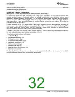
Because the voltage-error amplifier (VA) is a transconductance type of amplifier, the impedance on its input has
no bearing on the amplifier gain, which is determined solely by the product of its transconductance (gmv) with its
output impedance (ZOV). Thus the VSENSE input divider-network values are determined separately, based on
criteria discussed in the VINAC section. Its output is the VAO pin.
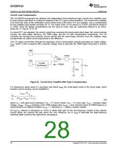
VAO
3V
+
VA
CZV
VSENSE
gmv = 70µS
CPV
RZV
Figure 23. Voltage Error Amplifier With Type II Compensation
The twice-line ripple voltage component of VSENSE must be sufficiently attenuated and phase-shifted at VAO to
achieve the desired level of 3rd-harmonic distortion of the input current wave-shape [4]. For every 1% of
3rd-harmonic input distortion allowable, the small-signal gain GVEA = VVAOpk / vSENSEpk = gmvxZOV at the twice-line
frequency should allow no more than 2% ripple over the full VAO voltage range. In the UCC28070, VVAO can
range from 1 V at zero load power to ~4.2 V(see note below) at full load power for a ΔVVAO = 3.2 V, so 2% of 3.2
V is 64-mV peak ripple.
NOTE
Although the maximum VAO voltage is clamped at 5 V, at full load VVAO may vary around
an approximate center point of 4.2 V to compensate for the effects of the quantized
feed-forward voltage in the multiplier stage (see Multiplier Section for details). Therefore,
4.2 V is the proper voltage to use to represent maximum output power when performing
voltage-loop gain calculations.
30
Copyright © 2010–2011, Texas Instruments Incorporated

 TI [ TEXAS INSTRUMENTS ]