UCC27423, UCC27424, UCC27425
www.ti.com
SLUS545D –NOVEMBER 2002–REVISED MAY 2013
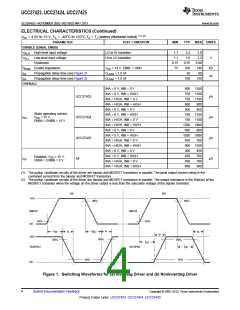
Two circuits are used to test the current capabilities of the UCC27423 driver. In each case external circuitry is
added to clamp the output near 5 V while the IC is sinking or sourcing current. An input pulse of 250 ns is
applied at a frequency of 1 kHz in the proper polarity for the respective test. In each test there is a transient
period where the current peaked up and then settled down to a steady-state value. The noted current
measurements are made at a time of 200 ns after the input pulse is applied, after the initial transient.
The first circuit in Figure 2 is used to verify the current sink capability when the output of the driver is clamped
around 5V, a typical value of gate-source voltage during the Miller plateau region. The UCC27423 is found to
sink 4.5A at VDD = 15V and 4.28A at VDD = 12V.
The circuit shown in Figure 3 is used to test the current source capability with the output clamped to around 5 V
with a string of Zener diodes. The UCC27423 is found to source 4.8 A at VDD = 15 V and 3.7 A at VDD = 12 V.
VDD
UCC27423
ENBA
1
2
3
4
ENBB
8
7
6
5
INPUT
D
SCHOTTKY
Ω
10
INA
OUTA
V
SUPPLY
5.5 V
C2
+
µ
1
F
F
GND
INB
VDD
OUTB
V
SNS
µ
100
F
R
0.1
µ
CER
SNS
1
F
AL EL
Ω
UDG-01065
Figure 3.
It should be noted that the current sink capability is slightly stronger than the current source capability at lower
VDD. This is due to the differences in the structure of the bipolar-MOSFET power output section, where the
current source is a P-channel MOSFET and the current sink has an N-channel MOSFET.
In a large majority of applications it is advantageous that the turn-off capability of a driver is stronger than the
turn-on capability. This helps to ensure that the MOSFET is held OFF during common power supply transients
which may turn the device back ON.
Parallel Outputs
The A and B drivers may be combined into a single driver by connecting the INA/INB inputs together and the
OUTA/OUTB outputs together. Then, a single signal can control the paralleled combination as shown in Figure 4.
Copyright © 2002–2013, Texas Instruments Incorporated
Submit Documentation Feedback
7
Product Folder Links: UCC27423 UCC27424 UCC27425

 TI [ TEXAS INSTRUMENTS ]