UCC27423, UCC27424, UCC27425
www.ti.com
SLUS545D –NOVEMBER 2002–REVISED MAY 2013
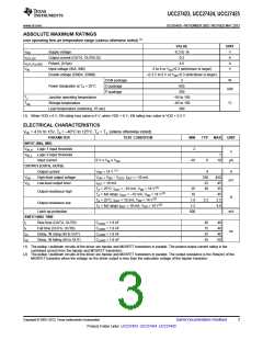
ABSOLUTE MAXIMUM RATINGS
over operating free-air temperature range (unless otherwise noted)
(1)
VALUE
UNIT
VDD
Supply voltage
-0.3 to 16
V
A
A
V
IOUT_DC
IOUT_PULSED
VIN
Output current (OUTA, OUTB) DC
Pulsed, (0.5μs)
0.2
4.5
Input voltage (INA, INB)
Enable voltage (ENBA, ENBB)
-5 to 6 or VDD+0.3 (whichever is larger)
–0.3 V to 6 V or VDD+0.3 (whichever is larger)
DGN package
D package
3
650
W
Power dissipation at TA = 25°C
mW
P package
350
TJ
Junction operating temperature
Storage temperature
–55 to 150
–65 to 150
300
Tstg
°C
Lead temperature (soldering, 10 sec)
(1) When VDD ≤ 6 V, EN rating max value is 6 V; when VDD > 6 V, EN rating max value is VDD + 0.3 V.
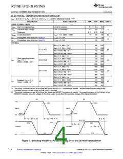
ELECTRICAL CHARACTERISTICS
VDD = 4.5V to 15V, TA = –40°C to 125°C ,TA = TJ, (unless otherwise noted)
PARAMETER
INPUT (INA, INB)
VIN_H Logic 1 input threshold
TEST CONDITION
MIN
2
TYP
MAX
UNIT
V
VIN_L
Logic 0 input threshold
Input current
1
0 V ≤ VIN ≤ VDD
–10
0
10
μA
OUTPUT (OUTA, OUTB)
(1)
Output current
VDD = 14 V
4
330
22
A
VOH
VOL
High-level output voltage
VOH = VDD – VOUT, IOUT = –10 mA
450
45
mV
Low-level output level
IOUT = 10 mA
TA = 25°C, IOUT = –10 mA, VDD = 14 V(2)
TA = full range, IOUT = –10 mA, VDD = 14 V(2)
TA = 25°C, IOUT = 10 mA, VDD = 14 V(2)
TA = full range IOUT = 10 mA, VDD = 14 V(2)
25
18
30
35
Output resistance high
45
Ω
1.9
1.2
500
2.2
2.5
4.0
Output resistance low
Latch-up protection
mA
SWITCHING TIME
tr
Rise time (OUTA, OUTB)
CLOAD = 1.8 nF
CLOAD = 1.8 nF
CLOAD = 1.8 nF
CLOAD = 1.8 nF
20
15
25
35
40
40
40
50
tf
Fall time (OUTA, OUTB)
Delay, IN rising (IN to OUT)
Delay, IN falling (IN to OUT)
ns
td1
td2
(1) The pullup / pulldown circuits of the driver are bipolar and MOSFET transistors in parallel. The pulsed output current rating is the
combined current from the bipolar and MOSFET transistors.
(2) The pullup / pulldown circuits of the driver are bipolar and MOSFET transistors in parallel. The output resistance is the Rds(on) of the
MOSFET transistor when the voltage on the driver output is less than the saturation voltage of the bipolar transistor.
Copyright © 2002–2013, Texas Instruments Incorporated
Submit Documentation Feedback
3
Product Folder Links: UCC27423 UCC27424 UCC27425

 TI [ TEXAS INSTRUMENTS ]