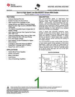
UCC27423, UCC27424, UCC27425
www.ti.com
SLUS545D –NOVEMBER 2002–REVISED MAY 2013
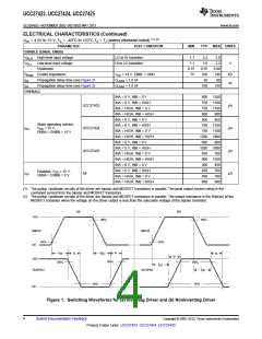
5V
ENBx
0V
V
V
IN_L
IN_H
t
t
D3
D4
V
DD
90%
90%
t
F
t
R
OUTx
10%
0V
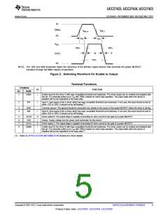
NOTE: The 10% and 90% thresholds depict the dynamics of the BiPolar output devices that dominate the power MOSFET
transition through the Miller regions of operation.
Figure 2. Switching Waveform for Enable to Output
Terminal Functions
TERMINAL
I/O
FUNCTION
NO.
NAME
1
ENBA
I
Enable input for the driver A with logic compatible threshold and hysteresis. The driver output can be enabled and disabled with
this pin. It is internally pulled up to VDD with 100kΩ resistor for active high operation. The output state when the device is
disabled will be low regardless of the input state.
2
INA
I
I
Input A. Input signal of the A driver which has logic compatible threshold and hysteresis. If not used, this input should be tied to
either VDD or GND. It should not be left floating.(1)
3
4
GND
INB
Common ground. This ground should be connected very closely to the source of the power MOSFET which the driver is driving.
Input B. Input signal of the A driver which has logic compatible threshold and hysteresis. If not used, this input should be tied to
either VDD or GND. It should not be left floating.
5
6
7
8
OUTB
VDD
O
I
Driver output B. The output stage is capable of providing 4A drive current to the gate of a power MOSFET.
Supply. Supply voltage and the power input connection for this device.
OUTA
ENBB
O
I
Driver output A. The output stage is capable of providing 4A drive current to the gate of a power MOSFET.
Enable input for the driver B with logic compatible threshold and hysteresis. The driver output can be enabled and disabled with
this pin. It is internally pulled up to VDD with 100kΩ resistor for active high operation. The output state when the device is
disabled will be low regardless of the input state.(1)
(1) Refer to APPLICATION INFORMATION Section for more details.
Copyright © 2002–2013, Texas Instruments Incorporated
Submit Documentation Feedback
5
Product Folder Links: UCC27423 UCC27424 UCC27425

 TI [ TEXAS INSTRUMENTS ]