UCC27423, UCC27424, UCC27425
www.ti.com
SLUS545D –NOVEMBER 2002–REVISED MAY 2013
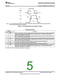
Figure 6.
In a power driver operating at high frequency, it is a significant challenge to get clean waveforms without much
overshoot/undershoot and ringing. The low output impedance of these drivers produces waveforms with high
di/dt. This tends to induce ringing in the parasitic inductances. Utmost care must be used in the circuit layout. It is
advantageous to connect the driver IC as close as possible to the leads. The driver IC layout has ground on the
opposite side of the output, so the ground should be connected to the bypass capacitors and the load with
copper trace as wide as possible. These connections should also be made with a small enclosed loop area to
minimize the inductance.
VDD
Although quiescent VDD current is very low, total supply current will be higher, depending on OUTA and OUTB
current and the programmed oscillator frequency. Total VDD current is the sum of quiescent VDD current and the
average OUT current. Knowing the operating frequency and the MOSFET gate charge (Qg), average OUT
current can be calculated from:
IOUT = Qg × f, where f is frequency
For the best high-speed circuit performance, two VDD bypass capacitors are recommended tp prevent noise
problems. The use of surface mount components is highly recommended. A 0.1μF ceramic capacitor should be
located closest to the VDD to ground connection. In addition, a larger capacitor (such as 1μF) with relatively low
ESR should be connected in parallel, to help deliver the high current peaks to the load. The parallel combination
of capacitors should present a low impedance characteristic for the expected current levels in the driver
application.
Drive Current and Power Requirements
The UCC27423/4/5 family of drivers are capable of delivering 4A of current to a MOSFET gate for a period of
several hundred nanoseconds. High peak current is required to turn the device ON quickly. Then, to turn the
device OFF, the driver is required to sink a similar amount of current to ground. This repeats at the operating
frequency of the power device. A MOSFET is used in this discussion because it is the most common type of
switching device used in high frequency power conversion equipment.
References 1 and 2 discuss the current required to drive a power MOSFET and other capacitive-input switching
devices. Reference 2 includes information on the previous generation of bipolar IC gate drivers.
When a driver IC is tested with a discrete, capacitive load it is a fairly simple matter to calculate the power that is
required from the bias supply. The energy that must be transferred from the bias supply to charge the capacitor
is given by:
1
2
2
E + CV
, where C is the load capacitor and V is the bias voltage feeding the driver.
Copyright © 2002–2013, Texas Instruments Incorporated
Submit Documentation Feedback
9
Product Folder Links: UCC27423 UCC27424 UCC27425

 TI [ TEXAS INSTRUMENTS ]