UCC27423, UCC27424, UCC27425
SLUS545D –NOVEMBER 2002–REVISED MAY 2013
www.ti.com
ELECTRICAL CHARACTERISTICS (Continued)
VDD = 4.5V to 15 V, TA = –40°C to 125°C,TA = TJ (unless otherwise noted)
(1) (2)
PARAMETER
ENABLE (ENBA, ENBB)
VIN_H High-level input voltage
TEST CONDITION
MIN
TYP
MAX UNITS
LO to HI transition
1.7
1.1
2.4
1.8
2.9
VIN_L
Low-level input voltage
Hysteresis
HI to LO transition
2.2
0.90
140
60
V
0.15
75
0.55
100
30
RENBL Enable impedance
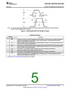
tD3 Propagation delay time (see Figure 2)
tD4 Propagation delay time (see Figure 2)
OVERALL
VDD = 14 V, ENBL = GND
CLOAD = 1.8 nF
kΩ
ns
CLOAD = 1.8 nF
100
150
INA = 0 V, INB = 0 V
900
750
750
600
300
750
750
1200
600
1050
450
900
300
450
450
600
1350
1100
1100
900
INA = 0 V, INB = HIGH
INA = HIGH, INB = 0 V
INA = HIGH, INB = HIGH
INA = 0 V, INB = 0 V
UCC27423
UCC27424
UCC27425
All
μA
μA
μA
μA
450
Static operating current,
VDD = 15 V,
ENBA = ENBB = 15 V
INA = 0 V, INB = HIGH
INA = HIGH, INB = 0 V
INA = HIGH, INB = HIGH
INA = 0 V, INB = 0 V
1100
1100
1800
900
IDD
INA = 0 V, INB = HIGH
INA = HIGH, INB = 0 V
INA = HIGH, INB = HIGH
INA = 0 V, INB = 0 V
1600
700
1350
450
INA = 0 V, INB = HIGH
INA = HIGH, INB = 0 V
INA = HIGH, INB = HIGH
700
Disabled, VDD = 15 V,
ENBA = ENBB = 0 V
IDD
700
900
(1) The pullup / pulldown circuits of the driver are bipolar and MOSFET transistors in parallel. The peak output current rating is the
combined current from the bipolar and MOSFET transistors.
(2) The pullup / pulldown circuits of the driver are bipolar and MOSFET transistors in parallel. The output resistance is the Rds(on) of the
MOSFET transistor when the voltage on the driver output is less than the saturation voltage of the bipolar transistor.
(a)
(b)
+5V
90%
90%
INPUT
INPUT
10%
10%
0V
t
t
t
t
f
t
F
D1
D2
F
t
F
16V
90%
90%
90%
t
D1
t
OUTPUT
OUTPUT
D2
10%
10%
0V
Figure 1. Switching Waveforms for (a) Inverting Driver and (b) Noninverting Driver
4
Submit Documentation Feedback
Copyright © 2002–2013, Texas Instruments Incorporated
Product Folder Links: UCC27423 UCC27424 UCC27425

 TI [ TEXAS INSTRUMENTS ]