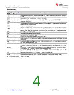
UCC21759-Q1
SLUSEB4A – AUGUST 2020 – REVISED DECEMBER 2020
www.ti.com
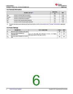
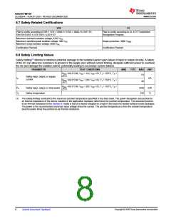
6.7 Safety-Related Certifications
VDE
UL
Plan to certify according to DIN V VDE V 0884-11 (VDE V 0884-11):2017-01;
DIN EN 61010-1 (VDE 0411-1):2011-07
Plan to certify according to UL 1577 Component
Recognition Program
Maximum transient isolation voltage, 4242 VPK
;
Maximum repetitive peak isolation voltage, 990 VPK
Maximum surge isolation voltage, 6000 VPK
;
Single protection, 3000 VRMS
Certification Planned
Certification Planned
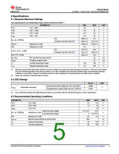
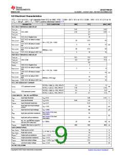
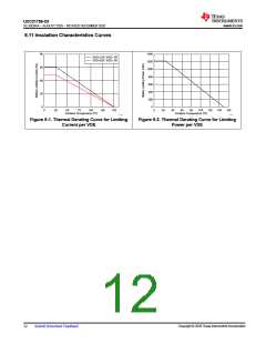
6.8 Safety Limiting Values
Safety limiting(1) intends to minimize potential damage to the isolation barrier upon failure of input or output circuitry. A failure
of the I/O can allow low resistance to ground or the supply and, without current limiting, dissipate sufficient power to overheat
the die and damage the isolation barrier, potentially leading to secondary system failures.
PARAMETER
TEST CONDITIONS
MIN
TYP
MAX UNIT
RθJA =68.3°C/W, VDD = 15V, VEE=-5V, TJ = 150°C, TA =
25°C
61
Safety input, output, or supply
current
IS
mA
49
RθJA =68.3°C/W, VDD = 20V, VEE=-5V, TJ = 150°C, TA =
25°C
RθJA =68.3°C/W, VDD = 20V, VEE=-5V, TJ = 150°C, TA =
25°C
PS
TS
Safety input, output, or total power
Safety temperature
1220
150
mW
°C
(1) The safety-limiting constraint is the maximum junction temperature specified in the data sheet. The power dissipation and junction-to-
air thermal impedance of the device installed in the application hardware determines the junction temperature. The assumed junction-
to-air thermal resistance in the Section 6.4 table is that of a device installed on a high-K test board for leaded surface-mount packages.
The power is the recommended maximum input voltage times the current. The junction temperature is then the ambient temperature
plus the power times the junction-to-air thermal resistance.
Copyright © 2020 Texas Instruments Incorporated
8
Submit Document Feedback

 TI [ TEXAS INSTRUMENTS ]