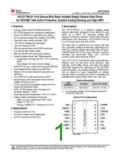
UCC21759-Q1
SLUSEB4A – AUGUST 2020 – REVISED DECEMBER 2020
www.ti.com
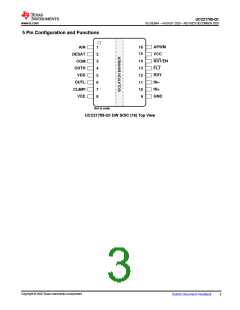
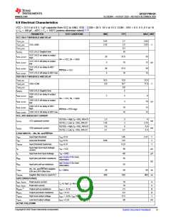
Pin Functions
PIN
I/O(1)
DESCRIPTION
NAME
NO.
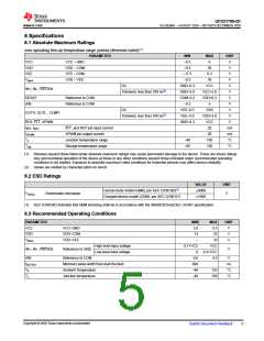
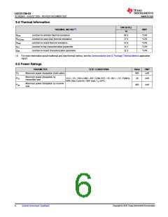
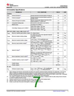
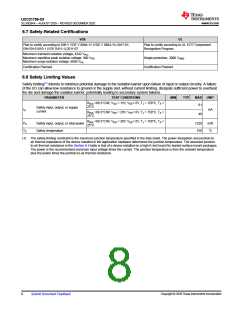
Isolated analog sensing input, parallel a small capacitor to COM for better noise immunity. If not used, short
to COM
AIN
1
I
DESAT
COM
2
3
4
I
Desaturation current protection input. If not used, short to COM
Common ground reference, connecting to emitter pin for IGBT or source pin for SiC-MOSFET
Gate driver output pull up
P
O
OUTH
Positive supply rail for gate drive voltage, Bypassing a >220nF capacitor to COM to support specified gate
driver source peak current capability
VDD
5
6
7
P
O
O
OUTL
CLMPI
Gate driver output pull down
Internal active Miller clamp, connecting this pin directly to the gate of the power transistor. If not used, short
to VEE
Negative supply rail for gate drive voltage. Bypassing a >220nF capacitor to COM to support specified gate
driver sink peak current capability
VEE
8
P
GND
IN+
9
P
I
Input power supply and logic ground reference
Non-inverting gate driver control input
10
11
IN–
I
Inverting gate driver control input. If not used, short to GND
Power good for VCC-GND and VDD-COM. RDY is open drain configuration and can be paralleled with other
RDY signals
RDY
FLT
12
13
O
O
Active low fault alarm output upon over current or short circuit detection. FLT is in open drain configuration
and can be paralleled with other faults
The RST/EN serves two purposes:
1) Enable / shutdown of the output side. The FET is turned off by a general turn-off, if terminal EN is set to
low;
RST/EN
14
I
2) Resets the DESAT condition signaled on FLT pin. if terminal RST/EN is set to low for more than 1000ns.
A reset of signal FLT is asserted at the rising edge of terminal RST/EN.
For automatic RESET function, this pin only serves as an EN pin. Enable / shutdown of the output side. The
FET is turned off by a general turn-off, if terminal EN is set to low.
VCC
15
16
P
Input power supply from 3V to 5.5V, bypassing a >100nF capacitor to GND
APWM
O
Isolated analog sensing PWM output. If not used, leave floating or tie a parallel capacitor to GND
(1) P = Power, G = Ground, I = Input, O = Output
Copyright © 2020 Texas Instruments Incorporated
4
Submit Document Feedback

 TI [ TEXAS INSTRUMENTS ]