UCC21759-Q1
SLUSEB4A – AUGUST 2020 – REVISED DECEMBER 2020
www.ti.com
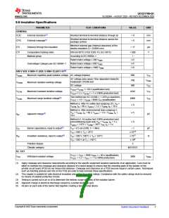
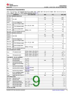
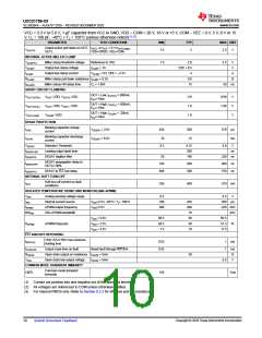
6.9 Electrical Characteristics
VCC = 3.3 V or 5.0 V, 1-µF capacitor from VCC to GND, VDD – COM = 20 V, 18 V or 15 V, COM – VEE = 0 V, 5 V, 8 V or 15
V, CL = 100 pF, –40°C < TJ < 150°C (unless otherwise noted)(1) (2)
.
PARAMETER
VCC UVLO THRESHOLD AND DELAY
VVCC_ON
TEST CONDITIONS
MIN
TYP
MAX UNIT
2.55
2.35
2.7
2.5
0.2
10
2.85
VVCC_OFF
VVCC_HYS
tVCCFIL
VCC–GND
2.65
V
VCC UVLO Deglitch time
VCC UVLO on delay to output
high
tVCC+ to OUT
tVCC– to OUT
tVCC+ to RDY
tVCC– to RDY
28
5
37.8
10
50
15
IN+ = VCC, IN– = GND
RST/EN = VCC
VCC UVLO off delay to output
low
µs
VCC UVLO on delay to RDY
high
30
5
37.8
10
50
15
VCC UVLO off delay to RDY low
VDD UVLO THRESHOLD AND DELAY
VVDD_ON
10.5
9.9
12.0
10.7
0.8
5
12.8
11.8
VVDD_OFF
VVDD_HYS
tVDDFIL
VDD–COM
V
VDD UVLO Deglitch time
VDD UVLO on delay to output
high
tVDD+ to OUT
tVDD– to OUT
tVDD+ to RDY
tVDD– to RDY
2
5
5
8
IN+ = VCC, IN– = GND
RST/EN = FLT=High
VDD UVLO off delay to output
low
10
µs
VDD UVLO on delay to RDY
high
10
10
15
15
VDD UVLO off delay to RDY low
VCC, VDD QUIESCENT CURRENT
OUT(H) = High, fS = 0Hz, AIN=2V
OUT(L) = Low, fS = 0Hz, AIN=2V
OUT(H) = High, fS = 0Hz, AIN=2V
OUT(L) = Low, fS = 0Hz, AIN=2V
2.5
1.45
3.6
3
2
4
2.75
5.9
IVCCQ
VCC quiescent current
VDD quiescent current
mA
mA
4
IVDDQ
3.1
3.7
5.3
LOGIC INPUTS — IN+, IN– and RST/EN
VINH
Input high threshold
Input low threshold
VCC=3.3V
VCC=3.3V
VCC=3.3V
1.85
1.52
0.33
2.31
V
V
V
VINL
0.99
VINHYS
Input threshold hysteresis
Input high level input leakage
current
IIH
VIN = VCC
VIN = GND
90
–90
55
µA
µA
IIL
Input low level input leakage
Input pins pull down resistance
see Section 8 for more
information
RIND
kΩ
see Section 8 for more
information
RINU
Input pins pull up resistance
55
IN+, IN– and RST/EN deglitch
(ON and OFF) filter time
TINFIL
fS = 50kHz
28
40
60
ns
ns
TRSTFIL
Deglitch filter time to reset /FLT
400
650
800
GATE DRIVER STAGE
IOUT, IOUTH Peak source current
IOUT, IOUTL
10
10
A
A
CL=0.18µF, fS=1kHz
Peak sink current
(3)
ROUTH
Output pull-up resistance
Output pull-down resistance
High level output voltage
Low level output voltage
IOUT = –0.1A
2.5
0.3
17.5
60
Ω
ROUTL
VOUTH
VOUTL
IOUT = 0.1A
Ω
IOUT = –0.2A, VDD=18V
IOUT = 0.2A
V
mV
ACTIVE PULLDOWN
Copyright © 2020 Texas Instruments Incorporated
Submit Document Feedback
9

 TI [ TEXAS INSTRUMENTS ]