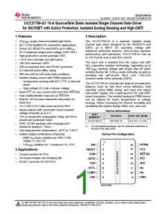
UCC21759-Q1
SLUSEB4A – AUGUST 2020 – REVISED DECEMBER 2020
www.ti.com
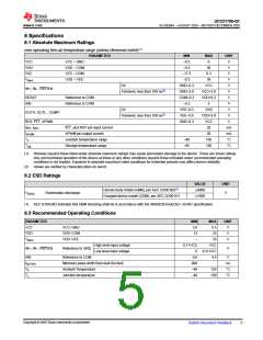
6 Specifications
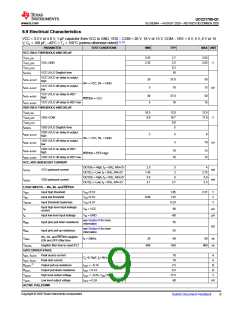
6.1 Absolute Maximum Ratings
over operating free-air temperature range (unless otherwise noted)(1)
PARAMETER
MIN
–0.3
MAX
6
UNIT
V
VCC
VDD
VEE
VMAX
VCC – GND
VDD – COM
VEE – COM
VDD – VEE
–0.3
36
V
–17.5
0.3
V
–0.3
36
V
DC
GND–0.3
GND–5.0
COM–0.3
–0.3
VCC
VCC+5.0
VDD+0.3
5
V
IN+, IN–, RST/EN
Transient, less than 100 ns(2)
V
DESAT
AIN
Reference to COM
Reference to COM
V
V
DC
VEE–0.3
VEE–5.0
GND–0.3
VDD
VDD+5.0
VCC
20
V
OUTH, OUTL , CLMPI
Transient, less than 100 ns(2)
V
RDY, FLT, APWM
V
IFLT, IRDY
IAPWM
TJ
FLT, and RDY pin input current
APWM pin output current
mA
mA
°C
°C
20
Junction temperature range
Storage temperature range
–40
–65
150
Tstg
150
(1) Stresses beyond those listed under absolute maximum ratings may cause permanent damage to the device. These are stress ratings
only and functional operation of the device at these or any other conditions beyond those indicated under recommended operating
conditions is not implied. Exposure to absolute-maximum-rated conditions for extended periods may affect device reliability.
(2) Values are verified by characterization on bench.
6.2 ESD Ratings
VALUE
±4000
±1500
UNIT
Human-body model (HBM), per AEC Q100-002(1)
Charged-device model (CDM), per AEC Q100-011
V(ESD)
Electrostatic discharge
V
(1) AEC Q100-002 indicates that HBM stressing shall be in accordance with the ANSI/ESDA/JEDEC JS-001 specification.
6.3 Recommended Operating Conditions
PARAMETER
VCC
MIN
MAX
5.5
UNIT
VCC–GND
VDD–COM
VDD–VEE
3.0
V
V
V
VDD
13
33
VMAX
–
0.7×VCC
0
33
High level input voltage
Low level input voltage
VCC
0.3×VCC
4.5
IN+, IN–, RST/EN
Reference to GND
V
AIN
tRST/EN
TA
Reference to COM
0.6
V
Minimum pulse width that reset the fault
Ambient Temperature
800
ns
°C
°C
–40
125
150
TJ
Junction temperature
–40
Copyright © 2020 Texas Instruments Incorporated
Submit Document Feedback
5

 TI [ TEXAS INSTRUMENTS ]