UCC21759-Q1
SLUSEB4A – AUGUST 2020 – REVISED DECEMBER 2020
www.ti.com
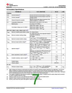
6.6 Insulation Specifications
PARAMETER
GENERAL
TEST CONDITIONS
VALUE
UNIT
CLR
CPG
External clearance(1)
Shortest terminal-to-terminal distance through air
> 8
> 8
mm
mm
Shortest terminal-to-terminal distance across the
package surface
External creepage(1)
Minimum internal gap (Internal clearance) of the
double insulation (2 × 0.0085 mm)
DTI
CTI
Distance through the insulation
> 17
µm
V
Comparative tracking index
Material group
DIN EN 60112 (VDE 0303-11); IEC 60112
According to IEC 60664–1
> 600
I
Rated mains voltage ≤ 300 VRMS
Rated mains voltage ≤ 600 VRMS
Rated mains voltage ≤ 1000 VRMS
I-IV
I-IV
I-III
Overvoltage Category per IEC 60664–1
DIN V VDE V 0884-11 (VDE V 0884-11):2017-01(2)
VIORM Maximum repetitive peak isolation voltage AC voltage (bipolar)
990
700
990
VPK
VRMS
VDC
AC voltage (sine wave) Time dependent dielectric
breakdown (TDDB) test
VIOWM
Maximum isolation working voltage
DC voltage
VTEST=VIOTM, t = 60 s (qualification test)
VTEST=1.2 x VIOTM, t = 1 s (100% production test)
VIOTM
Maximum transient isolation voltage
Maximum surge isolation voltage(3)
4242
VPK
VPK
Test method per IEC 62368-1, 1.2/50 µs waveform,
VTEST = 1.6 × VIOSM = 9600 VPK (qualification)
VIOSM
6000
≤ 5
Method a: After I/O safety test subgroup 2/3, Vini
VIOTM, tini = 60 s; Vpd(m) = 1.2 × VIORM, tm = 10 s
=
Method a: After environmental tests subgroup 1,
Vini = VIOTM, tini = 60 s; Vpd(m) = 1.6 × VIORM, tm
10 s
=
≤ 5
≤ 5
qpd
Apparent charge(4)
pC
Method b1: At routine test (100% production) and
preconditioning (type test) Vini = VIOTM, tini = 1 s;
Vpd(m) = 1.875 × VIORM = 3977 VPK, tm = 1 s
CIO
RIO
Barrier capacitance, input to output(5)
Insulation resistance, input to output(5)
VIO = 0.5 sin (2πft), f = 1 MHz
VIO = 500 V, TA = 25°C
~ 1
≥ 1012
≥ 1011
≥ 109
pF
Ω
VIO = 500 V, 100°C ≤ TA ≤ 125°C
VIO = 500 V at TS = 150°C
Pollution degree
Climatic category
2
40/125/21
UL 1577
VTEST = VISO = 3000 VRMS, t = 60 s (qualification);
VTEST = 1.2 × VISO, t = 1 s (100% production)
VISO
Withstand isolation voltage
3000
VRMS
(1) Apply creepage and clearance requirements according to the specific equipment isolation standards of an application. Care must be
taken to maintain the creepage and clearance distance of a board design to ensure that the mounting pads of the isolator on the
printed circuit board (PCB) do not reduce this distance. Creepage and clearance on a PCB become equal in certain cases. Techniques
such as inserting grooves and ribs on the PCB are used to help increase these specifications.
(2) This coupler is suitable for safe electrical insulation only within the safety ratings. Compliance with the safety ratings shall be ensured
by means of suitable protective circuits.
(3) Testing is carried out in air or oil to determine the intrinsic surge immunity of the isolation barrier.
(4) Apparent charge is electrical discharge caused by a partial discharge (pd).
(5) All pins on each side of the barrier tied together creating a two-terminal device
Copyright © 2020 Texas Instruments Incorporated
Submit Document Feedback
7

 TI [ TEXAS INSTRUMENTS ]