TUSB1310A
SLLSE32D–NOVEMBER 2010–REVISED MAY 2011
www.ti.com
3
FUNCTIONAL DESCRIPTION
3.1 Power On and Reset
The TUSB1310A has two hardware reset pins, a chip reset RESETN and a logic reset PHY_RESETN.
The RESETN is used only at Power On. The PHY_RESETN can be used as a functional reset. The ULPI
register also has a software reset.
Until all power sources are supplied, the OUT_ENABLE pin can control the output driver enable. After all
power sources are supplied, the chip reset RESETN and a ULPI soft reset will be asserted by the Link
Layer. The power up sequence is described in section 3.1.4
3.1.1 RESETN and PHY_RESETN – Hardware Reset
The RESETN sets all internal states to initial values. The Link Layer needs to hold the PHY in reset via
the RESETN until all power sources and the reference clock to the TUSB1310A are stable. All pins used
for strapping options must be set before RESETN de-assertion as they are latched by reset de-assertion.
All strapping option pins have internal pull-up or pull-down to set default values, but if any non-default
values are desired, they need to be controlled externally by the Link Layer Controller.
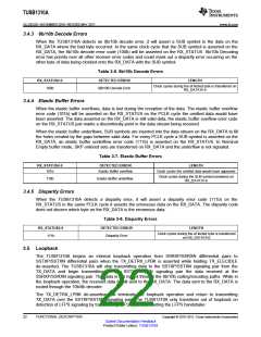
Table 3-1. Pin States in Chip Reset
PIPE CONTROL PIN NAME
TX_DETRX_LPBK
TX_ELECIDLE
TX_ONESZEROS
RX_POLARITY
POWER_DOWN
TX_MARGIN2-0
TX_DEEMP
STATE
Inactive
VALUE
0
1
Active
Inactive
0
Inactive
0
U2
10b
000b
1
Normal operating range
-3.5 dB
RATE
5.0 Gbps
1
TX_SWING
Full swing or half swing
Appropriate state
0 or 1
0 or 1
RX_TERMINATION
3.1.2 ULPI Reset – Software Reset
After power-up, the Link Layer Controller must set the Reset bit in ULPI register. It resets the core but
does not reset the ULPI interface or the ULPI registers.
During the ULPI reset, the ULPI_DIR is de-asserted. After the reset, the ULPI_DIR is asserted again and
the TUSB1310A sends an RX CMD update to the Link Layer. During the reset, the link should ignore
signals on the ULPI_DATA7-0 and must not access the TUSB1310A.
3.1.3 OUT_ENABLE - Output Enable
Digital IO buffers use two power supplies, core VDD1P1 and IO VDD1P8. During power up,
OUT_ENABLE must be asserted low for proper operation.
3.1.4 Power Up Sequence
The power up sequence is shown in Figure 3-1.
18
FUNCTIONAL DESCRIPTION
Copyright © 2010–2011, Texas Instruments Incorporated
Submit Documentation Feedback
Product Folder Link(s): TUSB1310A

 TI [ TEXAS INSTRUMENTS ]