TUSB1310A
SLLSE32D–NOVEMBER 2010–REVISED MAY 2011
www.ti.com
2.4 Clocking
Table 2-5. Clock Signal Name Description
SIGNAL NAME
TYPE
BALL NO.
DESCRIPTION
Crystal Input. This pin is the clock reference input for the TUSB1310A. The
XI
I
A12
TUSB1310A supports either a crystal unit, or a 1.8-V clock input. Frequencies
supported are 20, 25, 30, or 40 MHz.
XO
O
O
A11
D10
Crystal output. If a 1.8-V clock input is connected to XI, XO must be left open.
OOBCLK is driven in U3 mode.
CLKOUT
2.5 JTAG Interface
The JTAG Interface is used for board-level boundary scan. All digital IO support IEEE1149.1 boundary
scan and SuperSpeed differential pairs support IEEE1149.6 boundary scan.
Table 2-6. JTAG Signal Name Description
SIGNAL NAME
JTAG_TCK
TYPE
I, PU
I, PU
I, PU
I, PD
O
BALL NO.
G11
DESCRIPTION
JTAG test clock
JTAG_TMS
JTAG_TDI
D11
JTAG test mode select
JTAG test data input
E11
JTAG_TRSTN
JTAG_TDO
E12
JTAG test asynchronous reset. Active Low.
JTAG test data output
F11
2.6 Reset and Output Control Interface
Table 2-7. Reset and Output Control Signal Description
SIGNAL NAME
RESETN
TYPE
BALL NO.
DESCRIPTION
I
J11
Active Low. Resets the transmitter and receiver. This signal is asynchronous.
Active High. This can be connected to a 1.8-V power on reset signal on the PCB in
order to avoid static current and signal contention during power up.
0: Disable all driver outputs while IO powers are supplied, but internal control circuit
powers are not present during power up.
OUT_ENABLE
I
L10
1: Enable all driver outputs during normal operation.
2.7 Strap Options
Strapping pins are latched by reset de-assertion in the TUSB1310A.
Table 2-8. Strapping Options
SIGNAL NAME
XTAL_DIS
TYPE
BALL NO.
DESCRIPTION
Selects an input clock source
S, I/O, PD
F3
0
1
Crystal Input
Clock Input
(RX_ELECIDLE)
Spread spectrum clocking disable
SSC_DIS
(TX_MARGIN0)
S, I, PD
M9
E3
0
1
SSC enable
SSC disable
Selects PIPE
PIPE_16BIT
(PHY_STATUS)
S, I/O, PD
0
16-bit PIPE SDR mode
Must be 0 at reset.
14
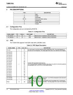
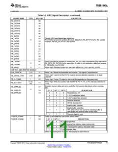
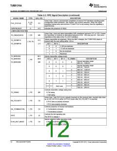
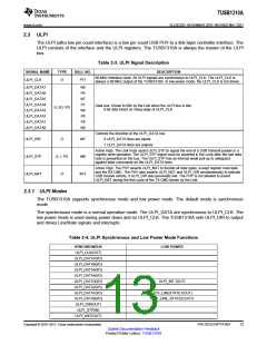
PIN DESCRIPTIONS
Copyright © 2010–2011, Texas Instruments Incorporated
Submit Documentation Feedback
Product Folder Link(s): TUSB1310A

 TI [ TEXAS INSTRUMENTS ]